TCET1103 Vishay, TCET1103 Datasheet

OPTOCOUPLER PHOTOTRANS 200% 4DIP

TCET1103

Manufacturer Part Number
TCET1103
Description
OPTOCOUPLER PHOTOTRANS 200% 4DIP
Manufacturer
Vishay
Datasheets

Specifications of TCET1103

Mounting Type
Through Hole
Isolation Voltage
5000 Vrms
Number Of Channels
1
Input Type
DC
Voltage - Isolation
5000Vrms
Current Transfer Ratio (min)
34% @ 1mA
Current Transfer Ratio (max)
200% @ 10mA
Voltage - Output
70V
Current - Output / Channel
50mA
Current - Dc Forward (if)
60mA
Vce Saturation (max)
300mV
Output Type
Transistor
Package / Case
4-DIP (0.300", 7.62mm)
Forward Current
60 mA
Maximum Input Diode Current
60 mA
Maximum Reverse Diode Voltage
6 V
Output Device
Transistor
Configuration
1
Maximum Collector Emitter Voltage
70 V
Maximum Collector Emitter Saturation Voltage
300 mV
Current Transfer Ratio
200 %
Maximum Forward Diode Voltage
1.6 V
Maximum Collector Current
50 mA
Maximum Power Dissipation
265 mW
Maximum Operating Temperature
+ 100 C
Minimum Operating Temperature
- 40 C
No. Of Channels
1
Optocoupler Output Type
Phototransistor
Input Current
50mA
Output Voltage
70V
Opto Case Style
DIP
No. Of Pins
4
Approval Bodies
VDE, CSA, BSI EN
Rohs Compliant
Yes
Lead Free Status / RoHS Status
Lead free / RoHS Compliant
Lead Free Status / RoHS Status
Lead free / RoHS Compliant, Lead free / RoHS Compliant

Available stocks

Company
Part Number
Manufacturer
Quantity
Price
Part Number:
TCET1103
Manufacturer:
Telefunk
Quantity:
15 045
Part Number:
TCET1103
Manufacturer:
FUJ
Quantity:
2 000
Part Number:
TCET1103
Manufacturer:
VISHAY
Quantity:
200
Part Number:
TCET1103
Manufacturer:
VISHAY/威世
Quantity:
20 000
Part Number:
TCET1103G
Manufacturer:
VISHAY
Quantity:
10 000
Part Number:
TCET1103G
Manufacturer:
VISHAY/威世
Quantity:
20 000
Company:
Part Number:
TCET1103G
Quantity:
70 000
Optocoupler, Phototransistor Output, High Temperature
Features
Agency Approvals
Applications
Switch-mode power supplies
Line receiver
Computer peripheral interface
Microprocessor system interface
Circuits for safe protective separation against electri-
cal shock according to safety class II (reinforced iso-
lation):
• For appl. class I - IV at mains voltage ≤ 300 V
• For appl. class I - III at mains voltage ≤ 600 V accord-
ing to DIN EN 60747-5-2(VDE0884)/ DIN EN 60747-
5-5 pending, table 2.
Description
The TCET110. consists of a phototransistor optically
coupled to a gallium arsenide infrared-emitting diode
in a 4-lead plastic dual inline package.
The elements are mounted on one leadframe using a
coplanar technique, providing a fixed distance
between input and output for highest safety require-
ments.
Isolation materials according to UL94-VO
Document Number 83503
Rev. 2.2, 05-Sep-06
• Extra low coupling capacity - typical 0.2 pF
• High Common Mode Rejection
• Low temperature coefficient of CTR
• CTR offered in 9 groups
• Reinforced Isolation provides circuit protection
• Lead-(Pb)-free component
• Component in accordance to RoHS 2002/95/EC
• UL1577, File No. E76222 System Code U, Double
• CSA 22.2 bulletin 5A, Double Protection
• BSI: EN 60065:2002, EN 60950:2000
• DIN EN 60747-5-2 (VDE0884)
• FIMKO
against electrical shock (Safety Class II)
and WEEE 2002/96/EC
Protection
Certificate No. 7081 and 7402
DIN EN 60747-5-5 pending
e3
Pollution degree 2 (DIN/VDE 0110 / resp. IEC 60664)
Climatic classification 55/100/21 (IEC 60068 part 1)
Rated impulse voltage (transient overvoltage)
V
Isolation test voltage (partial discharge test voltage)
V
Rated isolation voltage (RMS includes DC)
V
Rated recurring peak voltage (repetitive)
V
Thickness through insulation ≥ 0.75 mm
Internal creepage distance > 4 mm
Creepage current resistance according to VDE 0303/
IEC 112 Comparative Tracking Index:
CTI ≥ 175
VDE Standards
These couplers perform safety functions according to
the following equipment standards:
DIN EN 60747-5-2(VDE0884)/ DIN EN 60747-5-5
pending
Optocoupler for electrical safety requirements
IEC 60950/EN 60950
Office machines (applied for reinforced isolation for
mains voltage ≤ 400 VRMS)
VDE 0804
Telecommunication apparatus and data processing
IEC 60065
Safety for mains-operated electronic and related
household apparatus
17197_1
IOTM
pd
IOWM
IORM
= 1.6 kV
TCET1100/TCET1100G
A
= 8 kV peak
= 600 V
C
1
= 600 V
4
3
2
E
C
RMS
C
RMS
(848 V peak)
Vishay Semiconductors
D E
V
www.vishay.com
1

Related parts for TCET1103

TCET1103 Summary of contents

Page 1

... The elements are mounted on one leadframe using a coplanar technique, providing a fixed distance between input and output for highest safety require- ments. Isolation materials according to UL94-VO Document Number 83503 Rev. 2.2, 05-Sep-06 TCET1100/TCET1100G Vishay Semiconductors ...

Page 2

... CTR 130 - 260 %, DIP-4 TCET1109 CTR 200 - 400 %, DIP-4 TCET1100G CTR 50 - 600 %, DIP-4 TCET1101G CTR DIP-4 TCET1102G CTR 63 - 125 %, DIP-4 TCET1103G CTR 100 - 200 %, DIP-4 TCET1104G CTR 160 - 320 %, DIP-4 TCET1105G CTR 50 - 150 %, DIP-4 TCET1106G CTR 100 - 300 %, DIP-4 TCET1107G CTR 80 - 160 %, DIP-4 ...

Page 3

... The thermal model is represented in the thermal network below. Each resistance value given in this model can be used to calculate the tem- peratures at each node for a given operating condition. The thermal resistance from board to ambient will be dependent on the type of PCB, layout and thickness of copper traces. For a detailed explanation of the thermal model, please reference Vishay's Thermal Characteristics of Optocouplers Application note. ...

Page 4

... TCET1103G TCET1104 TCET1104G TCET1100 = TCET1100G TCET1105 TCET1105G TCET1106 TCET1106G TCET1107 TCET1107G TCET1108 TCET1108G TCET1109 TCET1109G TCET1101 = TCET1101G TCET1102 TCET1102G TCET1103 TCET1103G TCET1104 TCET1104G Min Typ. Max 1.25 1.6 50 Min Typ. Max 100 Min Typ. Max 0.3 110 0.3 Symbol Min Typ. ...

Page 5

... IO = 150 °C amb IOTM IOWM V IORM 0 150 125 13930 Figure 2. Test pulse diagram for sample test according to DIN EN 60747-5-2(VDE0884)/ DIN EN 60747-; IEC60747 Vishay Semiconductors Min Typ. Max 130 Min Typ. Max 265 Min Typ. Max 8 150 Min Typ. Max 1.6 8 1.3 ...

Page 6

... TCET1100/TCET1100G Vishay Semiconductors Switching Characteristics Parameter Delay time (see figure 3) Rise time (see figure 3) Turn-on time (see figure 3) Storage time (see figure 3) Fall time (see figure 3) Turn-off time (see figure 3) Turn-on time (see figure 4) Turn-off time (see figure mA; adjusted through 0.01 ...

Page 7

... Figure 9. Collector Dark Current vs. Ambient Temperature 100 0.1 0.01 2.0 1.4 1.6 1.8 95 11027 Figure 10. Collector Current vs. Forward Current 100 0 10985 Figure 11. Collector Current vs. Collector Emitter Voltage Vishay Semiconductors 100 Ambient Temperature (°C) amb 100 0 Forward Current (mA) ...

Page 8

... TCET1100/TCET1100G Vishay Semiconductors 1 0.8 CTR = 50 % 0.6 0.4 0 Collector Current (mA) 95 11028 C Figure 12. Collector Emitter Saturation Voltage vs. Collector Current 1000 100 Forward Current (mA) 95 11029 F Figure 13. Current Transfer Ratio vs. Forward Current 10 Non Saturated Operation 100 Ω off Collector Current (mA) 95 11030 C Figure 14 ...

Page 9

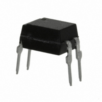
... Package Dimensions in mm Package Dimensions in mm Document Number 83503 Rev. 2.2, 05-Sep-06 TCET1100/TCET1100G Vishay Semiconductors 14789 14792 www.vishay.com 9 ...

Page 10

... Various national and international initiatives are pressing for an earlier ban on these substances. Vishay Semiconductor GmbH has been able to use its policy of continuous improvements to eliminate the use of ODSs listed in the following documents. 1. Annex A, B and list of transitional substances of the Montreal Protocol and the London Amendments respectively 2 ...

Page 11

... Information contained herein is intended to provide a product description only. No license, express or implied, by estoppel or otherwise, to any intellectual property rights is granted by this document. Except as provided in Vishay's terms and conditions of sale for such products, Vishay assumes no liability whatsoever, and disclaims any express or implied warranty, relating to sale and/or use of Vishay products including liability or warranties relating to fitness for a particular purpose, merchantability, or infringement of any patent, copyright, or other intellectual property right ...

Related keywords