TLP627(TP1,F,T) Toshiba, TLP627(TP1,F,T) Datasheet - Page 2
TLP627(TP1,F,T)
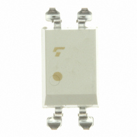
Manufacturer Part Number
TLP627(TP1,F,T)
Description
PHOTOCOUPLER DARL TRANS-OUT 4SMD
Manufacturer
Toshiba
Specifications of TLP627(TP1,F,T)
Number Of Channels
1
Input Type
DC
Voltage - Isolation
5000Vrms
Current Transfer Ratio (min)
1000% @ 1mA
Voltage - Output
300V
Current - Output / Channel
150mA
Current - Dc Forward (if)
60mA
Vce Saturation (max)
1.2V
Output Type
Darlington
Mounting Type
Surface Mount
Package / Case
4-SMD (300 mil)
Lead Free Status / RoHS Status
Lead free / RoHS Compliant
Current Transfer Ratio (max)
-
Other names
TLP627TP1FTR


Absolute Maximum Ratings
Recommended Operating Conditions
Operating Temperature Range
Storage Temperature Range
Lead Soldering Temperature (10s)
Total Package Power Dissipation
Total Package Power Dissipation Derating
Isolation Voltage
Note: Using continuously under heavy loads (e.g. the application of high temperature/current/voltage and the
(Note1)Device considered a two terminal device : LED side pins Shorted together and
Supply Voltage
Forward Current
Collector Current
Operating Temperature
Note: Recommended operating conditions are given as a design guideline to obtain expected performance of the
Forward Current
Forward Current Derating
Pulse Forward Current
Power Dissipation
Power Dissipation Derating (Ta≥25°C,1 Circuit)
Reverse Voltage
Junction Temperature
Collector-Emitter Voltage
Emitter -Collector Voltage
Collector Current
Collector Power Dissipation
Collector Power Dissipation Derating
Junction Temperature
significant change in temperature, etc.) may cause this product to decrease in the reliability significantly even
if the operating conditions (i.e. operating temperature/current/voltage, etc.) are within the absolute maximum
ratings.
Please design the appropriate reliability upon reviewing the Toshiba Semiconductor Reliability Handbook
(“Handling Precautions”/“Derating Concept and Methods”) and individual reliability data (i.e. reliability test
report and estimated failure rate, etc).
device. Additionally, each item is an independent guideline respectively. In developing designs using this
product, please confirm specified characteristics shown in this document.
together.
Characteristics
(AC,1min. , R.H.≤60%)
Characteristics
(Ta=25°C)
Symbol
V
T
I
I
CC
C
opr
F
(Ta≥25°C,1 Circuit)
(Ta≥25°C,1 Circuit)
Min.
−25
—
—
—
(1 Circuit)
(1 Circuit)
2
(Note1)
Typ.
16
—
—
—
∆ P
∆ P
Symbol
∆ P
∆I
Max.
200
120
V
V
T
BV
25
85
T
T
F
V
P
I
P
P
Tj
I
T
I
D
CEO
ECO
FP
c
sold
opr
C
stg
T
F
/°C
D
R
C
T
j
/°C
/°C
/°C
S
TLP627,TLP627-2,TLP627-4
Unit
mA
mA
−0.7(Ta≥39°C)
°C
V
*IF=20mA Max
-1.5(*-3.5)
-2.5(*-3.2)
150(*300)
250(*320)
TLP627
1(100μs pulse,100pps)
-1.0
100
60
260(10sec)
−55~100
−55~125
Rating
5000
125
300
150
125
0.3
DETECTOR side pins shorted
5
−0.5(Ta≥25°C)
TLP627-2
TLP627-4
-1.0
-0.7
100
150
-1.5
50
70
2007-10-01
mW /°C
mW /°C
mW /°C
mA /°C
V r m s
Unit
mW
mW
mW
mA
mA
°C
°C
°C
°C
°C
A
V
V
V
Related parts for TLP627(TP1,F,T)
Image
Part Number
Description
Manufacturer
Datasheet
Request
R

Part Number:
Description:
PHOTOCOUPLER HS DARL-OUT 4-DIP
Manufacturer:
Toshiba
Datasheet:

Part Number:
Description:
PHOTOCOUPLER DL HS DARL-OUT 8DIP
Manufacturer:
Toshiba
Datasheet:

Part Number:
Description:
PHOTOCOUPLER DARL TRANS-OUT 4SMD
Manufacturer:
Toshiba
Datasheet:
Part Number:
Description:
Transistor Output Optocouplers INCORRECT MOUSER P/N
Manufacturer:
Toshiba
Datasheet:
Part Number:
Description:
PHOTOCOUPLER DL HS DARL-OUT 8DIP
Manufacturer:
Toshiba
Datasheet:
Part Number:
Description:
PHOTOTRANSISTOR DUAL 8DIP SMD
Manufacturer:
Toshiba
Datasheet:

Part Number:
Description:
PHOTOCPLR QUAD HS DARL-OUT 16DIP
Manufacturer:
Toshiba
Datasheet:

Part Number:
Description:
OPTOCOUPLER, 5KV, TRANSISTOR O/P
Manufacturer:
Toshiba
Datasheet:


Part Number:
Description:
PHOTOCOUPLER QUAD HS DARL 16-DIP
Manufacturer:
Toshiba
Datasheet:
Part Number:
Description:
PHOTOCOUPLER DARL TRANS-OUT 4SMD
Manufacturer:
Toshiba
Datasheet: