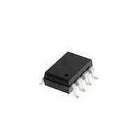
HCPL-7710#560 Avago Technologies US Inc., HCPL-7710#560 Datasheet - Page 14

HCPL-7710#560
Manufacturer Part Number
HCPL-7710#560
Description
OPTOCOUPLER 12MBD VDE 8-SMD
Manufacturer
Avago Technologies US Inc.
Datasheet
1.HCPL-7710-000E.pdf
(18 pages)
Specifications of HCPL-7710#560
Package / Case
8-SMD Gull Wing
Voltage - Isolation
3750Vrms
Number Of Channels
1, Unidirectional
Current - Output / Channel
10mA
Data Rate
12.5MBd
Propagation Delay High - Low @ If
20ns
Input Type
Logic
Output Type
Push-Pull, Totem-Pole
Mounting Type
Surface Mount, Gull Wing
Isolation Voltage
3750 Vrms
Maximum Continuous Output Current
10 mA
Maximum Fall Time
8 ns
Maximum Forward Diode Current
10 mA
Maximum Rise Time
9 ns
Output Device
Logic Gate Photo IC
Configuration
1 Channel
Maximum Baud Rate
12.5 MBps
Maximum Power Dissipation
150 mW
Maximum Operating Temperature
+ 100 C
Minimum Operating Temperature
- 40 C
Lead Free Status / RoHS Status
Contains lead / RoHS non-compliant
Available stocks
Company
Part Number
Manufacturer
Quantity
Price
14
Isolated Node with Transceiver Powered by the Network
Figure 20 shows a node powered by both the network
and another source. In this case, the transceiver and
isolated (network) side of the two optocouplers are
powered by the network. The rest of the node is
powered by the AC line which is very beneficial when
an application requires a significant amount of power.
This method is also desirable as it does not heavily load
the network.
More importantly, the unique “dual-inverting” design
of the HCPL-x710 ensure the network will not “lock-up”
if either AC line power to the node is lost or the node
powered-off. Specifically, when input power (V
the HCPL-x710 located in the transmit path is eliminat-
ed, a RECESSIVE bus state is ensured as the HCPL-x710
output voltage (V
Figure 20. Isolated node with transceiver powered by the network.
DRAIN/SHIELD
SIGNAL
POWER
NETWORK
SUPPLY
POWER
O
) go HIGH.
NODE/APP SPECIFIC
HCPL
0710
TRANSCEIVER
* OPTIONAL FOR BUS V + SENSE
uP/CAN
HCPL-0710 fig 19
HCPL
0710
DD1
NON ISO
HCPL
REG.
0710
5 V
) to
AC LINE
V+ (SIGNAL)
V– (SIGNAL)
V+ (POWER)
V– (POWER)
*Bus V+ Sensing
It is suggested that the Bus V+ sense block shown in
Figure 20 be implemented. A locally powered node with
an un-powered isolated Physical Layer will accumulate
errors and become bus-off if it attempts to transmit. The
Bus V+ sense signal would be used to change the BOI
attribute of the DeviceNet Object to the “auto-reset”
(01) value. Refer to Volume 1, Section 5.5.3. This would
cause the node to continually reset until bus power was
detected. Once power was detected, the BOI attribute
would be returned to the “hold in bus-off” (00) value.
The BOI attribute should not be left in the “auto-reset”
(01) value since this defeats the jabber protection ca-
pability of the CAN error confinement. Any inexpensive
low frequency optical isolator can be used to implement
this feature.
GALVANIC
ISOLATION
BOUNDARY


