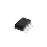
HCPL-2503#500 Avago Technologies US Inc., HCPL-2503#500 Datasheet - Page 11

HCPL-2503#500
Manufacturer Part Number
HCPL-2503#500
Description
OPTOCOUPLER 1MBS 8-SMD
Manufacturer
Avago Technologies US Inc.
Datasheet
1.HCPL-2503500.pdf
(12 pages)
Specifications of HCPL-2503#500
Input Type
DC
Package / Case
8-SMD Gull Wing
Voltage - Isolation
3750Vrms
Number Of Channels
1, Unidirectional
Current - Output / Channel
8mA
Data Rate
250kbps
Propagation Delay High - Low @ If
1µs @ 8mA
Current - Dc Forward (if)
25mA
Output Type
Open Collector
Mounting Type
Surface Mount, Gull Wing
Isolation Voltage
3750 Vrms
Output Device
Phototransistor
Configuration
1 Channel
Current Transfer Ratio
22 %
Maximum Baud Rate
1 MBps
Maximum Forward Diode Voltage
1.7 V
Maximum Reverse Diode Voltage
5 V
Maximum Input Diode Current
25 mA
Maximum Power Dissipation
100 mW
Maximum Operating Temperature
+ 70 C
Minimum Operating Temperature
0 C
Lead Free Status / RoHS Status
Contains lead / RoHS non-compliant
Available stocks
Company
Part Number
Manufacturer
Quantity
Price
V
Figure 7. Test circuit for transient immunity and typical waveforms
Figure 8. Recommended circuits
Recommended Operation
The HCPL-2503 optocoupler is specified for use in LSTTL-
to-LSTTL and TTL-to-LSTTL interfaces. The recommended
circuits show the interface design and give suggested
component values. The input current I
a nominal value and a range. The range in I
from the tolerances in V
The CTR of the optocoupler is given as the minimum
CM
7404
74LS04
7405
74LS05
0 V
V
V
O
O
SWITCH AT A: I = 0 mA
SWITCH AT B: I = 16 mA
A
10 V
V
t
R
r
CC1
IN
10%
A) TYPICAL NON-INVERTING CIRCUIT
I
F
90%
1
2
3
4
F
F
HCPL-2503
10%
CC
and the input resistor R
90%
t
r
, t
t
8
7
6
5
f
f
= 8 ns
5 V
V
OL
F
I
is given as both
O
R
V
L
HCPL-2503 fig 7
FF
V
B
B
CC2
74LS04
74LS05
HCPL-2503 fig 8
F
A
results
IN
I
.
F
7405
74LS05
initial value over temperature, taken directly from the
Electrical Specifications. The value given for I
based on the minimum CTR and the minimum I
worst case values for R
has ample design margin, allowing more than 20% for
CTR degradation even under these worst case condi-
tions. For additional information on CTR degradation
see Application Note 1002.
1
2
3
4
A
R
IN
V
CC1
PULSE GEN.
HP 8007
I
+
F
B) TYPICAL INVERTING CIRCUIT
V
CM
–
1
2
3
4
(SEE NOTE 10)
HCPL-2503
8
7
6
5
L
and V
8
7
6
5
CC
R
L
. The resulting I
I
O
R
+5 V
V
L
O
V
B
CC2
74LS04
74LS05
OL
(min) is
OL
F
using
(min)


