TLP718(F) Toshiba, TLP718(F) Datasheet

IC PHOTOCOUPLER IRED 6-SDIP

TLP718(F)

Manufacturer Part Number
TLP718(F)
Description
IC PHOTOCOUPLER IRED 6-SDIP
Manufacturer
Toshiba
Datasheet

Specifications of TLP718(F)

Voltage - Isolation
5000Vrms
Number Of Channels
1, Unidirectional
Current - Output / Channel
25mA
Propagation Delay High - Low @ If
120ns @ 0 ~ 3mA
Current - Dc Forward (if)
20mA
Input Type
DC
Output Type
Push-Pull, Totem-Pole
Mounting Type
Through Hole
Package / Case
6-SDIP (0.300", 7.62mm)
Configuration
1 Channel
Maximum Forward Diode Voltage
1.7 V
Maximum Reverse Diode Voltage
5 V
Maximum Operating Temperature
+ 100 C
Minimum Operating Temperature
- 40 C
Isolation Voltage
5000 Vrms
Maximum Fall Time
30 ns
Maximum Rise Time
30 ns
Output Device
Logic Gate Photo IC
Lead Free Status / RoHS Status
Lead free / RoHS Compliant
Other names
TLP718F
TLP718F
Isolated Bus Drivers
High Speed Line Receivers
Microprocessor System Interfaces
integrated high-gain, high-speed photodetector. This unit is a 6-pin SDIP. The
TLP718 is 50% smaller than the 8-PIN DIP and meets the reinforced insulation
class requirements of international safety standards. Therefore the mounting
area can be reduced in equipment requiring safety standard certification.
driving. The detector IC has an internal shield that provides a guaranteed
common-mode transient immunity of 10 kV / μs.
line-up.
Truth Table
The Toshiba TLP718 consists of a GaAℓAs light-emitting diode and an
The TLP718 is inverter logic type. For buffer logic type, the TLP715 is in
The detector has a totem pole output stage to provide both source and sink
Inverter logic type (totem pole output)
Guaranteed performance over temperature : −40 to 100°C
Power supply voltage : 4.5 to 20 V
Input current: I FHL = 3mA (Max.)
Switching time ( t pHL / t pLH) : 250 ns (Max.)
Common-mode transient immunity : ±10 kV/μs (Min)
Isolation voltage : 5000 Vrms (Min)
UL recognized
c-UL recognized
Option (D4)
Construction Mechanical Rating
Maximum Operating Insulation Voltage : 890V
Highest Permissible Over Voltage
(Note) : When a EN60747-5-2 approved type is needed,
Creepage Distance
Clearance
Insulation Thickness
TÜV recognized / VDE under application : DIN EN60747-5-2
UL1577, File No.E67349
CSA Component Acceptance Service No. 5A, File No.E67349
Input
H
L
Please designate “Option(D4)”
OFF
LED
ON
OFF
Tr1
ON
TOSHIBA PHOTOCOUPLER GaAℓAs IRED & PHOTO-IC
7.62 mm pitch
standard type
7.0 mm (Min)
7.0 mm (Min)
0.4 mm (Min)
OFF
Tr2
ON
Output
H
L
: 8000V
TLP718
10.16 mm pitch
TLPXXXF type
8.0 mm (Min)
8.0 mm (Min)
0.4 mm (Min)
PK
PK
1
1+
3-
0.1 μF bypass capacitor must be
connected between pins 6 and 4. (Note 5)
VF
Pin Configuration (Top View)
Schematic
1
2
3
SHIELD
I
F
Weight:0.26 g (t yp .)
SHIELD
TOSHIBA
4.58±0.25
1 2 3
6 5 4
0.4±0.1
1.27±0.2
VCC
GND
4
6
5
11-5J1
1:ANODE
2:N.C.
3:CATHODE
4:GND
5:Vo (Output)
6:Vcc
2009-04-20
7.62±0.25
Tr1
Tr2
1.25±0.25
9.7±0.3
TLP718
Unit in mm
I
CC
I
11-5J1
O
4
5
6
V
GND
V
CC
O

Related parts for TLP718(F)

TLP718(F) Summary of contents

Page 1

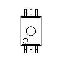
... Isolated Bus Drivers High Speed Line Receivers Microprocessor System Interfaces The Toshiba TLP718 consists of a GaAℓAs light-emitting diode and an integrated high-gain, high-speed photodetector. This unit is a 6-pin SDIP. The TLP718 is 50% smaller than the 8-PIN DIP and meets the reinforced insulation class requirements of international safety standards ...

Page 2

... Please design the appropriate reliability upon reviewing the Toshiba Semiconductor Reliability Handbook (“Handling Precautions”/“Derating Concept and Methods”) and individual reliability data (i.e. reliability test report and estimated failure rate, etc). ...

Page 3

Electrical Characteristics (Unless otherwise specified, Ta =−40 to 100°C, V CHARACTERISTIC SYMBOL Input forward voltage V F Temperature coefficient of ΔV F /ΔTa forward voltage Input reverse current I R Input capacitance C T Logic LOW output voltage V OL ...

Page 4

Switching Characteristics (Unless otherwise specified −40 to 100°C, V CHARACTERISTIC SYMBOL Propagation delay time to logic HIGH output Propagation delay time to logic LOW output Switching time dispersion between ON and OFF Rise Time (10 – ...

Page 5

TEST CIRCUIT 7: Switching Time Test Circuit mA(P.G) (f=50 kHz , duty=50% less than 5ns Vcc GND SHIELD CL: stray capacitance of probe and wiring (to 15 pF) TEST CIRCUIT 8: ...

Page 6

... Product shall not be used for or incorporated into any products or systems whose manufacture, use, or sale is prohibited under any applicable laws or regulations. • The information contained herein is presented only as guidance for Product use. No responsibility is assumed by TOSHIBA for any infringement of patents or any other intellectual property rights of third parties that may result from the use of Product. No license to any intellectual property right is granted by this document, whether express or implied, by estoppel or otherwise. • ...

Related keywords