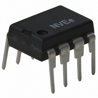
IL612A-2E NVE, IL612A-2E Datasheet - Page 9

IL612A-2E
Manufacturer Part Number
IL612A-2E
Description
ISOLATOR TX/RX CMOS 8DIP
Manufacturer
NVE
Series
IsoLoop®r
Datasheet
1.IL610A-1E.pdf
(17 pages)
Specifications of IL612A-2E
Inputs - Side 1/side 2
1/1
Number Of Channels
2
Isolation Rating
2500Vrms
Voltage - Supply
3 V ~ 5.5 V
Data Rate
10Mbps
Propagation Delay
20ns
Output Type
Open Drain
Package / Case
8-DIP
Operating Temperature
-40°C ~ 85°C
No. Of Channels
2
Supply Current
2mA
Supply Voltage Range
3V To 5.5V
Digital Ic Case Style
DIP
No. Of Pins
8
Operating Temperature Range
-40°C To +85°C
Rohs Compliant
Yes
Lead Free Status / RoHS Status
Lead free / RoHS Compliant
Other names
390-1089-5
Available stocks
Company
Part Number
Manufacturer
Quantity
Price
Company:
Part Number:
IL612A-2E
Manufacturer:
NVE Corp/Isolation Products
Quantity:
135
In the non-inverting circuit, the In terminal is
connected via a 1 k current-limiting resistor to the
supply rail, and the input is connected to the In+
terminal. Assume the supply voltage is +5 V and the
input signal is a 5 V CMOS signal. A 1 k resistance
is selected to limit the coil current to 5 mA. For the
purpose of this illustration we will ignore the coil
resistance. When a logic high (+5 V) is applied to the
input, the current through the coil is zero. When the
input is a logic low (0 V), approximately 5 mA flows
through the coil from the In side to the In+ side.
Figure 4 shows that the device will transition to both
logic states easily under these conditions. Now
assume that the 5 V rail is at 5.5 V and the CMOS
input signal is loaded so that its high level is only
4.5 V. When a logic high (4.5 V) appears on the
input, there is still a current of 1mA flowing
through the coil. Figure 4 shows that the device is
getting close to the off-state threshold of 1.5 mA,
and now exceeds the specification of 0.5 mA for
this logic level. Some intermittent operation or
complete non-function should be expected in this
case. The designer must ensure that the difference
between the logic high voltage and the power supply
voltage is such that the residual current in the coil is
lower than 0.5 mA.
The inverting configuration design problem is similar
to the problems associated with standard logic. In the
inverting configuration, the signal into the coil is
differential with respect to ground. The designer
must ensure that the difference between the logic low
voltage and the coil ground is such that the residual
coil current is less than 0.5 mA. Conventional ground
bounce design precautions apply.
The IL612A does not offer inverting operation because the coil In inputs are internally hardwired to the device power supply.
Therefore it is important to ensure the isolator power supply is at the same voltage as the power supply to the source of the input
logic signal.
IL600 devices are simple to use as long as it is remembered that there must be enough coil current (5 mA) to ensure logic low
output, and close to zero current (0.5 mA to 0 mA) to ensure logic high output.
Figure 5. Inverting and Non-Inverting circuits
Inverting Circuit
Inverting Circuit
Non-Inverting Circuit
Non-Inverting Circuit
Data In
Data In
Data In
Data In
9
1K
1K
GND
GND
C
C
C
C
boost
boost
+5 V
+5 V
1K
1K
boost
boost
GND
GND
1
1
2
2
3
3
+5 V
+5 V
IL610A
IL610A
1
1
+
+
-
-
2
2
3
3
IL610A
IL610A
+
+
-
-
IL600A Series
GND
GND
8
8
6
6
5
5
C
C
GND
GND
2
2
8
8
Data Out
Data Out
6
6
5
5
1
1
R
R
C
C
Note. C
Note. C
2
2
L
L
Note. C
Note. C
Data Out
Data Out
1
1
V
V
R
R
DD
DD
L
L
1
1
V
V
1
1
is 47 nF ceramic.
is 47 nF ceramic.
DD
DD
is 47 nF ceramic.
is 47 nF ceramic.


