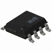
IL612-3E NVE, IL612-3E Datasheet - Page 5

IL612-3E
Manufacturer Part Number
IL612-3E
Description
ISOLATOR TX/RX CMOS 8SOIC
Manufacturer
NVE
Series
IsoLoop®r
Datasheet
1.IL610-1E.pdf
(21 pages)
Specifications of IL612-3E
Inputs - Side 1/side 2
1/1
Number Of Channels
2
Isolation Rating
2500Vrms
Voltage - Supply
3 V ~ 5.5 V
Data Rate
100Mbps
Propagation Delay
12ns
Output Type
CMOS
Package / Case
8-SOIC (3.9mm Width)
Operating Temperature
-40°C ~ 85°C
No. Of Channels
2
Supply Current
2mA
Supply Voltage Range
3V To 5.5V
Digital Ic Case Style
SOIC
No. Of Pins
8
Operating Temperature Range
-40°C To +85°C
Rohs Compliant
Yes
Lead Free Status / RoHS Status
Lead free / RoHS Compliant
Other names
390-1088-5
Available stocks
Company
Part Number
Manufacturer
Quantity
Price
Company:
Part Number:
IL612-3E
Manufacturer:
NVE
Quantity:
7 451
Electrical Specifications
Electrical specifications are T
Notes:
Parameters
Coil Input Impedance
Temperature Coefficient
of Coil Resistance
Input Threshold for Output Logic High
Input Threshold for Output Logic Low
Quiescent Current
Logic High Output Voltage
Logic Low Output Voltage
Logic Output Drive Current
Failsafe Operation Input Current
Input Signal Rise and Fall Times
Data Rate
Minimum Pulse Width
Propagation Delay Input to Output
(High-to-Low)
Propagation Delay Input to Output
(Low to High)
Average Propagation Delay Drift
Pulse Width Distortion |t
Pulse Jitter
Propagation Delay Skew
Output Rise Time (10–90%)
Output Fall Time (10–90%)
Common Mode Transient Immunity
1.
2.
3.
4.
5.
Failsafe Operation is defined as the guaranteed output state which will be achieved if the DC input current falls between the input levels specified
(see Test Circuit for details).
Minimum Pulse Width is the shortest pulse width at which the specified PWD is guaranteed.
PWD is defined as | t
66,535-bit pseudo-random binary signal (PRBS) NRZ bit pattern with no more than five consecutive 1s or 0s; 800 ps transition time.
t
PSK
(4)
is equal to the magnitude of the worst case difference in t
(2)
PHL
(5)
−t
PHL −
min
PLH
to T
|
t
(3)
(1)
PLH
max
|.
and 4.5 V to 5.5 V unless otherwise stated.
|CM
IL612, I
IL612, I
IL614, I
IL614, I
IL610, I
IL611, I
IL613, I
TC R
Symbol
I
I
FS-HIGH
Z
FS-LOW
PWD
t
V
V
I
IR
PW
t
t
t
t
H
I
|I
PHL
PLH
PLH
PSK
COIL
INH
INL
t
t
t
|,|CM
, t
OH
OL
O
R
F
J
COIL
|
IF
DD1
DD2
DD1
DD2
DD
DD
DD
L
Switching Specifications at 5V
|
PHL
Min.
−25
100
0.5
4.9
4.0
and/or t
10
−2
15
5
7
5
5
PLH
that will be seen between units at 25°C.
Typ.
85||9
0.2
3.5
4.8
0.2
10
10
20
1
2
4
2
2
6
2
4
5
0
8
8
3
2
2
Max.
0.25
100
0.1
0.8
0.5
25
15
15
3
6
3
3
9
3
6
1
5
2
4
4
Ω||nH
kV/µs
Units
Mbps
ps/°C
Ω/°C
IL600 Series
mA
mA
mA
mA
mA
mA
mA
mA
mA
mA
mA
mA
µs
ns
ns
ns
ps
ns
ns
ns
ns
V
V
Test Conditions
T
V
V
Single or Differential
V
Single or Differential
V
V
V
V
V
V
See Test Circuit 1
See Test Circuit 1
See Test Circuit 1
See Test Circuit 1
See Test Circuit 1
See Test Circuit 1
See Test Circuit 1
See Test Circuit 1
See Test Circuit 1
See Test Circuit 1
See Test Circuit 1
V
AMB
DD
DD
DD
DD
DD
DD
DD
DD
DD
T
= 300 V
= 3.0 V to 5.5 V
= 3.0 V to 5.5 V
= 3.0 V to 5.5 V
= 3.0 V to 5.5 V
= 5 V, I
= 5 V, I
= 5 V, I
= 5 V, I
= 5 V, I
= 25°C
peak
IN
O
O
O
O
= 20 µA
= 4 mA
= −20 µA
= −4 mA
= 0


