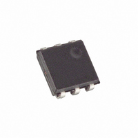
DS2413P+ Maxim Integrated Products, DS2413P+ Datasheet

DS2413P+
Specifications of DS2413P+
Related parts for DS2413P+
DS2413P+ Summary of contents
Page 1
... High ESD Immunity of 1-Wire IO Pin: 8kV HBM Typical TSOC and TDFN Packages Available ORDERING INFORMATION DS2413P+ LED R1 DS2413P+T&R DS2413Q+T& Denotes a lead(Pb)-free package/RoHS-compliant package. Local Switch Power T&R = Tape and reel. PIN CONFIGURATION ...
Page 2
ABSOLUTE MAXIMUM RATINGS Voltage on Any Pin to GND Maximum Current into IO Pin Maximum Current into PIO Pin Maximum Current Through GND Pins (Both Pins Tied Together) Operating Temperature Range Junction Temperature Storage Temperature Range Lead Temperature (soldering, 10s) ...
Page 3
PARAMETER SYMBOL Presence Detect Sample t MSP Time (Notes 1, 20) IO PIN, 1-Wire WRITE Write-0 Low Time t W0L (Notes 1, 17) Write-1 Low Time t W1L (Notes 1, 17) IO PIN, 1-Wire READ Read Low Time t RL ...
Page 4
PARAMETER STANDARD SPEED MIN t (incl 61µs SLOT REC t 480µs RSTL t 15µs PDH t 60µs PDL t 60µs W0L PIN DESCRIPTION NAME TSOC PIN # TDFN PIN # IO 2 PIOA 6 PIOB 4 GND1 1 ...
Page 5
LASERED ROM Each DS2413 has a unique ROM Registration Number that is 64 bits long, as shown in Figure 3. The first eight bits are a 1-Wire family code. The next 48 bits are a unique serial number. The ...
Page 6
PIO STUCTURE Each PIO consists of an open-drain pulldown transistor with 28V capability. The transistor is controlled by the PIO Output Latch, as shown in Figure 5. The PIO Control unit connects the PIOs to the 1-Wire interface. Figure 5. ...
Page 7
Figure 6. PIO Function Flow Chart Bus Master TX Memory Function Command F5h PIO Access Read? Note 1) See the command description for the exact timing of the PIO pin sampling and updating. DS2413 Samples PIO Pin Status Bus Master ...
Page 8
PIO ACCESS WRITE [5Ah] The PIO Access Write command writes to the PIO output latches, which control the pulldown transistors of the PIO channels endless loop this command first writes new data to the PIO and then reads ...
Page 9
The idle state for the 1-Wire bus is high. If for any reason a transaction needs to be suspended, the bus MUST be left in the idle state if the transaction is to resume. If this does not occur and ...
Page 10
SEARCH ROM [F0h] When a system is initially brought up, the bus master might not know the number of devices on the 1-Wire bus or their device ID numbers. By taking advantage of the wired-AND property of the bus, the ...
Page 11
Figure 10-1. ROM Functions Flow Chart From PIO Functions Flow Chart (Figure 6) Bus Master TX ROM Function Command 33h N Read ROM Command ? DS2413 TX Family Code (1 Byte) DS2413 TX Serial Number (6 ...
Page 12
Figure 10-2. ROM Functions Flow Chart (continued Figure 10, 1 Part From Figure Part Command ? From Figure Part To Figure Part A5h 3Ch N Resume Overdrive Skip ROM ...
Page 13
SIGNALING The DS2413 requires strict protocols to ensure data integrity. The protocol consists of four types of signaling on one line: Reset Sequence with Reset Pulse and Presence Pulse, Write-Zero, Write-One, and Read-Data. Except for the Presence pulse, the ...
Page 14
Read/Write Time Slots Data communication with the DS2413 takes place in time slots, which carry a single bit each. Write-time slots transport data from bus master to slave. Read-time slots transfer data from slave to master. Figure 12 illustrates the ...
Page 15
Master-to-Slave For a write-one time slot, the voltage on the data line must have crossed the V low time t is expired. For a write-zero time slot, the voltage on the data line must stay below the V W1LMAX threshold ...
Page 16
Figure 13. Noise Suppression Scheme V PUP Case A 0V COMMAND-SPECIFIC 1-Wire COMMUNICATION PROTOCOL—LEGEND SYMBOL RST 1-Wire Reset Pulse generated by master. PD 1-Wire Presence Pulse generated by slave. Select Command and data to satisfy the ...
Page 17
PIO ACCESS READ EXAMPLE Read the state of the PIOs 3 times. With only a single DS2413 connected to the bus master, the communication looks like this: MASTER MODE PIO ACCESS WRITE EXAMPLE ...
Page 18
... Maxim/Dallas Semiconductor cannot assume responsibility for use of any circuitry other than circuitry entirely embodied in a Maxim/Dallas Semiconductor product. No circuit patent licenses are implied. Maxim/Dallas Semiconductor reserves the right to change the circuitry and specifications without notice at any time MAXIM is a registered trademark of Maxim Integrated Products, Inc. DALLAS is a registered trademark of Dallas Semiconductor Corporation. DESCRIPTION . ...


