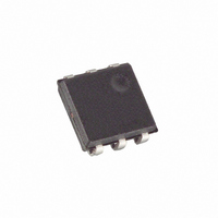
DS2401P+ Maxim Integrated Products, DS2401P+ Datasheet - Page 5

DS2401P+
Manufacturer Part Number
DS2401P+
Description
IC SILICON SERIAL NUMBER 6-TSOC
Manufacturer
Maxim Integrated Products
Specifications of DS2401P+
Applications
*
Mounting Type
Surface Mount
Package / Case
6-TSOC
Data Bus Width
64 bit
Interface Type
1-Wire
Maximum Operating Current
5 uA
Maximum Operating Temperature
+ 85 C
Minimum Operating Temperature
- 40 C
Mounting Style
SMD/SMT
Supply Voltage (max)
6 V
Supply Voltage (min)
2.8 V
Ic Function
Silicon Serial Number IC
Supply Voltage Range
2.8V To 6V
Operating Temperature Range
-40°C To +85°C
Digital Ic Case Style
TSOC
No. Of Pins
6
Filter Terminals
SMD
Rohs Compliant
Yes
Lead Free Status / RoHS Status
Lead free / RoHS Compliant
DS2401
1-Wire SIGNALING
The DS2401 requires a strict protocol to ensure data integrity. The protocol consists of four types of
signaling on one line: reset sequence with Reset Pulse and Presence Pulse, write 0, write 1, and read data.
All these signals except Presence Pulse are initiated by the bus master.
The initialization sequence required to begin any communication with the DS2401 is shown in Figure 5.
A reset pulse followed by a Presence Pulse indicates the DS2401 is ready to send or receive data given
the correct ROM command.
, minimum 480 μ s). The bus master then releases the
The bus master transmits (T
) a reset pulse (t
X
RSTL
). The 1-Wire bus is pulled to a high state via the 5k Ω pullup resistor.
line and goes into receive mode (R
X
, 15-60 μ s) and then transmits the
After detecting the rising edge on the data pin, the DS2401 waits (t
PDH
, 60-240 μ s). The 1-Wire bus requires a pullup resistor range of 1.5k Ω to 5k Ω ,
Presence Pulse (t
PDL
depending on bus load characteristics.
READ/WRITE TIME SLOTS
The definitions of write and read time slots are illustrated in Figure 6. All time slots are initiated by the
master driving the data line low. The falling edge of the data line synchronizes the DS2401 to the master
by triggering a delay circuit in the DS2401. During write time slots, the delay circuit determines when the
DS2401 will sample the data line. For a read data time slot, if a “0” is to be transmitted, the delay circuit
determines how long the DS2401 will hold the data line low overriding the “1” generated by the master.
If the data bit is a 1, the DS2401 will leave the read data time slot unchanged.
5 of 10


