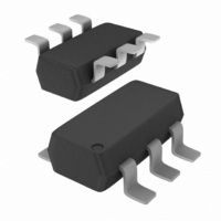
NCP1729SN35T1G ON Semiconductor, NCP1729SN35T1G Datasheet - Page 6

NCP1729SN35T1G
Manufacturer Part Number
NCP1729SN35T1G
Description
IC INVERTER SWITCHED CAP 6TSOP
Manufacturer
ON Semiconductor
Type
Switched Capacitor (Charge Pump), Invertingr
Datasheet
1.NCP1729SN35T1.pdf
(22 pages)
Specifications of NCP1729SN35T1G
Internal Switch(s)
Yes
Synchronous Rectifier
No
Number Of Outputs
1
Voltage - Output
-1.15 ~ -5.5 V, 2.3 ~ 11 V
Current - Output
50mA
Frequency - Switching
35kHz
Voltage - Input
1.15 ~ 5.5 V
Operating Temperature
-40°C ~ 85°C
Mounting Type
Surface Mount
Package / Case
SC-74-6
Power - Output
313mW
Function
Inverting
Output Voltage
- 5.5 V to - 1.15 V
Output Current
100 mA
Maximum Operating Temperature
+ 150 C
Mounting Style
SMD/SMT
Operating Supply Voltage (min)
1.15V
Operating Supply Voltage (max)
5.5V
Package Type
TSOP
Pin Count
6
Mounting
Surface Mount
Lead Free Status / RoHS Status
Lead free / RoHS Compliant
Other names
NCP1729SN35T1GOS
NCP1729SN35T1GOS
NCP1729SN35T1GOSTR
NCP1729SN35T1GOS
NCP1729SN35T1GOSTR
Available stocks
Company
Part Number
Manufacturer
Quantity
Price
Part Number:
NCP1729SN35T1G
Manufacturer:
ON/安森美
Quantity:
20 000
Capacitor Selection
output ripple voltage, it is recommended that low ESR
capacitors be used. Additionally, larger values of C
lower the output resistance and larger values of C
reduce output voltage ripple. (See Equation 3).
corresponding output resistance values at 25°C. Table 2
shows the output voltage ripple for various values of C
and C
calculated.
Input Supply Bypassing
reduce AC impedance and minimize noise effects due to the
switching internals in the device. If the device is loaded from
Table 1. Output Resistance vs. Capacitance
(C
Table 2. Output Voltage Ripple vs. Capacitance
(C
In order to maintain the lowest output resistance and
Table 1 shows various values of C
The input voltage, V
1
1
= C
= C
3
C
. The data in Tables 1 and 2 was measured not
1
C
2
2
= C
1
= C
= C
= C
0.68
0.68
2
(mF)
1.3
3.3
7.3
1.3
3.3
7.3
10
24
50
10
24
50
3
3
= C
2
), V
), V
= C
3
in
in
(mF)
3
= 4.75 V and V
= 4.75 V and V
in
should be capacitively bypassed to
Output Voltage Ripple
out
out
1
, C
= −4.0 V
= −4.0 V
R
2
out
(mV)
55.4
36.9
26.0
25.8
25.5
25.0
24.0
322
205
120
and C
69
56
32
20
(W)
3
with the
http://onsemi.com
2
1
1
will
will
, C
NCP1729
2
6
V
(at least equal to C
device is loaded from V
between the pins is sufficient.
Voltage Inverter
voltage inverter (Figure 14). This application uses two or
three external capacitors. The C
(output capacitor) are required. The input bypass capacitor
C
output is equal to −V
Refer to Tables 1 and 2 for capacitor selection. The test setup
used for the majority of the characterization is shown in
Figure 14.
Layout Considerations
practice is recommended. Mount components as close
together as possible to minimize stray inductance and
capacitance. Also use a large ground plane to minimize
noise leakage into other circuitry.
Capacitor Resources
switching loss. Low ESR capacitors are recommended. The
NCP1729 was characterized using the capacitors listed in
Table 3. This list identifies low ESR capacitors for the
voltage inverter application.
Table 3. Capacitor Types
AVX
843−448−9411
www.avxcorp.com
Cornell Dubilier
508−996−8561
www.cornell−dubilier.com
Sanyo/Os−con
619−661−6835
www.sanyovideo.com/oscon.htm
Vishay
603−224−1961
www.vishay.com
out
3
The most common application for a charge pump is the
As with any switching power supply circuit, good layout
Selecting the proper type of capacitor can reduce
, may be necessary depending on the application. The
to GND, it is recommended that a large value capacitor
Manufacturer/Contact
1
) be connected from V
in
plus any voltage drops due to loading.
in
to V
out
, a small (0.7 mF) capacitor
1
(pump capacitor) and C
Part Types/Series
in
ESRD
to GND. If the
593D
TPS
SVP
594
SN
2


