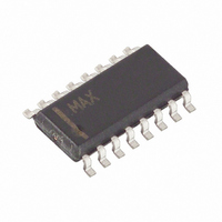
MAX797CSE+T Maxim Integrated Products, MAX797CSE+T Datasheet - Page 13

MAX797CSE+T
Manufacturer Part Number
MAX797CSE+T
Description
IC CNTRLR STEP DOWN 16-SOIC
Manufacturer
Maxim Integrated Products
Type
Step-Down (Buck)r
Datasheet
1.MAX797CSE.pdf
(32 pages)
Specifications of MAX797CSE+T
Internal Switch(s)
No
Synchronous Rectifier
Yes
Number Of Outputs
2
Voltage - Output
3.3V, 5V, Adj
Current - Output
10A
Frequency - Switching
150kHz, 300kHz
Voltage - Input
4.5 ~ 30 V
Operating Temperature
0°C ~ 70°C
Mounting Type
Surface Mount
Package / Case
16-SOIC (3.9mm Width)
Power - Output
696mW
Lead Free Status / RoHS Status
Lead free / RoHS Compliant
PWM Controller Blocks:
Bias Generator Blocks:
These internal IC blocks aren’t powered directly from
the battery. Instead, a +5V linear regulator steps down
the battery voltage to supply both the IC internal rail (VL
pin) as well as the gate drivers. The synchronous-
switch gate driver is directly powered from +5V VL,
while the high-side-switch gate driver is indirectly pow-
ered from VL via an external diode-capacitor boost cir-
cuit. An automatic bootstrap circuit turns off the +5V
linear regulator and powers the IC from its output volt-
age if the output is above 4.5V.
The heart of the current-mode PWM controller is a
multi-input open-loop comparator that sums three sig-
nals: output voltage error signal with respect to the ref-
erence voltage, current-sense signal, and slope
compensation ramp (Figure 3). The PWM controller is a
direct summing type, lacking a traditional error amplifi-
er and the phase shift associated with it. This direct-
summing configuration approaches the ideal of
cycle-by-cycle control over the output voltage.
Under heavy loads, the controller operates in full PWM
mode. Each pulse from the oscillator sets the main
PWM latch that turns on the high-side switch for a peri-
od determined by the duty factor (approximately
V
nous rectifier latch is set. 60ns later the low-side switch
turns on, and stays on until the beginning of the next
clock cycle (in continuous mode) or until the inductor
current crosses zero (in discontinuous mode). Under
fault conditions where the inductor current exceeds the
100mV current-limit threshold, the high-side latch
resets and the high-side switch turns off.
At light loads (SKIP = low), the inductor current fails to
exceed the 30mV threshold set by the minimum-current
comparator. When this occurs, the controller goes into
idle mode, skipping most of the oscillator pulses in
order to reduce the switching frequency and cut back
gate-charge losses. The oscillator is effectively gated
off at light loads because the minimum-current com-
parator immediately resets the high-side latch at the
OUT
• Multi-Input PWM Comparator
• Current-Sense Circuit
• PWM Logic Block
• Dual-Mode Internal Feedback Mux
• Gate-Driver Outputs
• Secondary Feedback Comparator
• +5V Linear Regulator
• Automatic Bootstrap Switchover Circuit
• +2.505V Reference
/V
IN
). As the high-switch turns off, the synchro-
______________________________________________________________________________________
Synchronous Rectifier for CPU Power
PWM Controller Block
Step-Down Controllers with
Table 3. Operating-Mode Truth Table
beginning of each cycle, unless the feedback signal
falls below the reference voltage level.
When in PWM mode, the controller operates as a fixed-
frequency current-mode controller where the duty ratio
is set by the input/output voltage ratio. The current-
mode feedback system regulates the peak inductor
current as a function of the output voltage error signal.
Since the average inductor current is nearly the same
as the peak current, the circuit acts as a switch-mode
transconductance amplifier and pushes the second
output LC filter pole, normally found in a duty-factor-
controlled (voltage-mode) PWM, to a higher frequency.
To preserve inner-loop stability and eliminate regenera-
tive inductor current “staircasing,” a slope-compensa-
tion ramp is summed into the main PWM comparator to
reduce the apparent duty factor to less than 50%.
The relative gains of the voltage- and current-sense
inputs are weighted by the values of current sources
that bias three differential input stages in the main PWM
comparator (Figure 4). The relative gain of the voltage
comparator to the current comparator is internally fixed
at K = 2:1. The resulting loop gain (which is relatively
low) determines the 2.5% typical load regulation error.
The low loop-gain value helps reduce output filter
capacitor size and cost by shifting the unity-gain
crossover to a lower frequency.
* MAX796/MAX799 have no SKIP pin and therefore can’t go
X = Don’t Care
SHDN
High
High
High
High
into low-noise mode.
Low
SKIP
High
Low
Low
Low
X
CURRENT
Medium,
LOAD
<10%
<30%
>30%
High,
Low,
X
X
Low Noise*
Shutdown
MODE
(PWM)
NAME
PWM
Idle
Idle
All circuit blocks
turned off; supply
current = 1µA typ
Pulse-skipping;
supply current =
700µA typ at V
10V; discontinuous
inductor current
Pulse-skipping;
continuous inductor
current
Constant-frequency
PWM; continuous
inductor current
Constant-frequency
PWM regardless of
load; continuous
inductor current
even at no load
DESCRIPTION
IN
=
13


