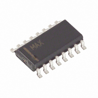
MAX797CSE Maxim Integrated Products, MAX797CSE Datasheet - Page 22

MAX797CSE
Manufacturer Part Number
MAX797CSE
Description
IC CONTRLR STEP-DOWN PWM 16-SOIC
Manufacturer
Maxim Integrated Products
Type
Step-Down (Buck)r
Datasheet
1.MAX797CSE.pdf
(32 pages)
Specifications of MAX797CSE
Internal Switch(s)
No
Synchronous Rectifier
Yes
Number Of Outputs
2
Voltage - Output
3.3V, 5V, Adj
Current - Output
10A
Frequency - Switching
150kHz, 300kHz
Voltage - Input
4.5 ~ 30 V
Operating Temperature
0°C ~ 70°C
Mounting Type
Surface Mount
Package / Case
16-SOIC (3.9mm Width)
Power - Output
696mW
Output Voltage
5 V
Output Current
10 A
Switching Frequency
340 KHz
Maximum Operating Temperature
+ 70 C
Mounting Style
SMD/SMT
Minimum Operating Temperature
0 C
Supply Current
0.44 mA
Case
sop
Dc
99+
Lead Free Status / RoHS Status
Contains lead / RoHS non-compliant
Available stocks
Company
Part Number
Manufacturer
Quantity
Price
Company:
Part Number:
MAX797CSE
Manufacturer:
MAXIM
Quantity:
9 800
Part Number:
MAX797CSE
Manufacturer:
MAXIM/美信
Quantity:
20 000
Company:
Part Number:
MAX797CSE+
Manufacturer:
Maxim
Quantity:
300
Company:
Part Number:
MAX797CSE+T
Manufacturer:
MAXIM
Quantity:
3
Company:
Part Number:
MAX797CSE-T
Manufacturer:
SP
Quantity:
226
Part Number:
MAX797CSE-T
Manufacturer:
MAXIM/美信
Quantity:
20 000
The two high-current N-channel MOSFETs must be
logic-level types with guaranteed on-resistance specifi-
cations at V
better (i.e., 2V max rather than 3V max). Drain-source
breakdown voltage ratings must at least equal the max-
imum input voltage, preferably with a 20% derating fac-
tor. The best MOSFETs will have the lowest
on-resistance per nanocoulomb of gate charge.
Multiplying R
by which to compare various MOSFETs. Newer MOS-
FET process technologies with dense cell structures
generally give the best performance. The internal gate
drivers can tolerate >100nC total gate charge, but
70nC is a more practical upper limit to maintain best
switching times.
In high-current applications, MOSFET package power
dissipation often becomes a dominant design factor.
I
both high- and low-side MOSFETs. I
tributed between Q1 and Q2 according to duty factor
(see the equations below). Switching losses affect the
upper MOSFET only, since the Schottky rectifier clamps
the switching node before the synchronous rectifier
turns on. Gate-charge losses are dissipated by the dri-
ver- er and don’t heat the MOSFET. Ensure that both
MOSFETs are within their maximum junction tempera-
ture at high ambient temperature by calculating the
temperature rise according to package thermal-resis-
tance specifications. The worst-case dissipation for the
high-side MOSFET occurs at the minimum battery volt-
age, and the worst-case for the low-side MOSFET
occurs at the maximum battery voltage.
where: On-state voltage drop V
Under output short circuit, the synchronous-rectifier
MOSFET suffers extra stress and may need to be over-
sized if a continuous DC short circuit must be tolerated.
Step-Down Controllers with
Synchronous Rectifier for CPU Power
22
______Selecting Other Components
2
R power losses are the greatest heat contributor for
PD (upper FET) = I
PD (lower FET) = I
______________________________________________________________________________________
C
I
20ns = DH driver inherent rise/fall time
GATE
RSS
+ V
DUTY = (V
GS
DS(ON)
IN
= MOSFET reverse transfer capacitance
= DH driver peak output current capability
= 4.5V. Lower gate threshold specs are
x I
(1A typically)
LOAD
x Q
OUT
LOAD 2
LOAD 2
G
x f x
+ V
provides a meaningful figure
(
Q2
x R
––––––––––– +20ns
x R
V
) / (V
Q_
MOSFET Switches
IN
DS(ON)
I
DS(ON)
GATE
x C
= I
IN
2
LOAD
R losses are dis-
RSS
- V
x (1 - DUTY)
x DUTY
Q1
x R
)
DS(ON)
)
During short circuit, Q2’s duty factor can increase to
greater than 0.9 according to:
where the on-state voltage drop V
x R
Rectifier D1 is a clamp that catches the negative induc-
tor swing during the 110ns dead time between turning
off the high-side MOSFET and turning on the low-side.
D1 must be a Schottky type in order to prevent the
lossy parasitic MOSFET body diode from conducting. It
is acceptable to omit D1 and let the body diode clamp
the negative inductor swing, but efficiency will drop one
or two percent as a result. Use an MBR0530 (500mA
rated) type for loads up to 1.5A, a 1N5819 type for
loads up to 3A, or a 1N5822 type for loads up to 10A.
D1’s rated reverse breakdown voltage must be at least
equal to the maximum input voltage, preferably with a
20% derating factor.
A signal diode such as a 1N4148 works well for D2 in
most applications. If the input voltage can go below 6V,
use a small (20mA) Schottky diode for slightly improved
efficiency and dropout characteristics. Don’t use large
power diodes such as 1N5817 or 1N4001, since high
junction capacitance can cause VL to be pumped up to
excessive voltages.
The secondary diode in coupled-inductor applications
must withstand high flyback voltages greater than 60V,
which usually rules out most Schottky rectifiers.
Common silicon rectifiers such as the 1N4001 are also
prohibited, as they are far too slow. This often makes
fast silicon rectifiers such as the MURS120 the only
choice. The flyback voltage across the rectifier is relat-
ed to the V
former turns ratio:
where: N is the transformer turns ratio SEC/PRI
Subtract the main output voltage (V
in this equation if the secondary winding is returned to
V
rating must also accommodate any ringing due to leak-
age inductance. D3’s current rating should be at least
twice the DC load current on the secondary output.
OUT
Q2 DUTY (short circuit) = 1 - [V
DS(ON).
and not to ground. The diode reverse breakdown
V
V
SEC
OUT
V
FLYBACK
IN
is the maximum secondary DC output voltage
-V
is the primary (main) output voltage
(Transformer Secondary Diode)
OUT
= V
difference according to the trans-
SEC
Boost-Supply Diode D2
+ (V
Rectifier Diode D1
Rectifier Diode D3
IN
Q2
Q
- V
OUT
= (120mV / R
/ (V
OUT
) from V
IN(MAX)
) x N
FLYBACK
- V
SENSE
Q1
)]
)


