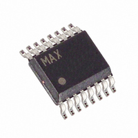
MAX1705EEE+T Maxim Integrated Products, MAX1705EEE+T Datasheet - Page 11

MAX1705EEE+T
Manufacturer Part Number
MAX1705EEE+T
Description
IC DC-DC CONV LN 16-QSOP
Manufacturer
Maxim Integrated Products
Type
Step-Up (Boost)r
Datasheet
1.MAX1706EEE.pdf
(18 pages)
Specifications of MAX1705EEE+T
Internal Switch(s)
Yes
Synchronous Rectifier
No
Number Of Outputs
1
Voltage - Output
2.5 ~ 5.5 V
Current - Output
850mA
Frequency - Switching
300kHz
Voltage - Input
0.7 ~ 5.5 V
Operating Temperature
-40°C ~ 85°C
Mounting Type
Surface Mount
Package / Case
16-QSOP
Power - Output
696mW
Lead Free Status / RoHS Status
Lead free / RoHS Compliant
Figure 2. Typical Operating Circuit (PFM Mode)
The step-up switching DC-DC converter generates an
adjustable output to supply both power circuitry (such
as RF power amplifiers) and the internal low-dropout
linear regulator. During the first part of each cycle, the
internal n-channel MOSFET switch is turned on. This
allows current to ramp up in the inductor and store
energy in a magnetic field. During the second part of
each cycle, when the MOSFET is turned off, the voltage
across the inductor reverses and forces current
through the diode and synchronous rectifier to the out-
put filter capacitor and load. As the energy stored in
the inductor is depleted, the current ramps down, and
the output diode and synchronous rectifier turn off.
Voltage across the load is regulated using either PWM
or PFM operation, depending on the CLK/SEL pin set-
ting (Table 1).
When CLK/SEL is pulled high, the MAX1705/MAX1706
operate in a high-power, low-noise PWM mode. During
PWM operation, they switch at a constant frequency
(300kHz), and modulate the MOSFET switch pulse
width to control the power transferred per cycle and
regulate the voltage across the load. In PWM mode, the
Step-Up DC-DC Converters with Linear Regulator
NOTE: HEAVY LINES INDICATE HIGH-CURRENT PATH.
(TO PGND)
Low-Noise, High-Power PWM Operation
INPUT 0.9V TO 3.6V
______________________________________________________________________________________
C7
22µF
R6
1- to 3-Cell, High-Current, Low-Noise,
R5
0.33µF
C8
(TO OUT)
Step-Up Converter
L1 10µH (22µH)
LBP
LBN
REF
ONA
ONB
CLK/SEL
LBO
MAX1705
MAX1706
100kΩ
GND
R7
LX
TRACK
FBLDO
POUT
PGND
OUT
LDO
FB
devices can output up to 850mA. Switching harmonics
generated by fixed-frequency operation are consistent
and easily filtered.
During PWM operation, each of the internal clock’s ris-
ing edges sets a flip-flop, which turns on the n-channel
MOSFET switch (Figure 3). The switch is turned off
when the sum of the voltage-error and current-
feedback signals trips a multi-input comparator and
resets the flip-flop; the switch remains off for the rest of
the cycle. When a change occurs in the output voltage
error signal into the comparator, it shifts the level that
the inductor current is allowed to ramp to during each
cycle and modulates the MOSFET switch pulse width.
A second comparator enforces a 1.55A (max) inductor-
Table 1. Selecting the Operating Mode
D1
(200kHz to 400kHz)
165kΩ
100kΩ
External Clock
R3
R4
CLK/SEL
C9
0.33µF
0
1
C3
0.1µF
C2*
*OPTIONAL.
( ) ARE FOR MAX1706.
100kΩ
191kΩ
R2
R1
Synchronized
MODE
PFM
PWM
PWM
C5*
0.33µF
BOOST OUTPUT 3.6V
LDO OUTPUT 3.3V
C1*
(TO PGND)
Low supply current
Low noise,
high output current
Low noise,
high output current
C6
22µF
FEATURES
C4
220µF
(100µF)
11


