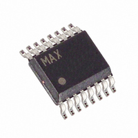
MAX686EEE+T Maxim Integrated Products, MAX686EEE+T Datasheet - Page 13

MAX686EEE+T
Manufacturer Part Number
MAX686EEE+T
Description
IC SUPPLY LCD BIAS INV 16-QSOP
Manufacturer
Maxim Integrated Products
Type
Step-Up (Boost), Invertingr
Datasheet
1.MAX686EEE.pdf
(16 pages)
Specifications of MAX686EEE+T
Internal Switch(s)
Yes
Synchronous Rectifier
No
Number Of Outputs
1
Voltage - Output
±27.5V
Current - Output
100mA
Frequency - Switching
300kHz
Voltage - Input
2.7 ~ 5.5 V
Operating Temperature
-40°C ~ 85°C
Mounting Type
Surface Mount
Package / Case
16-QSOP
Power - Output
667mW
Lead Free Status / RoHS Status
Lead free / RoHS Compliant
Parallel a feed-forward capacitor (C
pensate the feedback loop and ensure stability (Figure
4). Use values up to 100pF for most applications.
Choose the lowest capacitor value that ensures stability;
high capacitance values may degrade line regulation.
The output can be adjusted with a potentiometer
instead of the DAC (Figure 5). Choose R
and connect it between REF and GND. Connect R3 to
the potentiometer’s wiper instead of to DACOUT. Use
the same design equations for adjusting the output volt-
age with the DAC.
When the voltage at POK is greater than 1.125V (typical),
the open-drain LCDON output pulls low. LCDON can
withstand up to 27.5V to control an external PNP transis-
tor to switch on the MAX686’s positive output (Figures 6
and 7). A PFET can also be used, but a resistor-divider
must be used in conjunction with it, so that the PFET does
not exceed its V
this feature are as follows:
• An off-switch driver to ensure that a positive boosted
Figure 6. Using the POK for Input Voltage Monitoring
V
TO 27.5V
IN
output goes to 0V during shutdown. Connect POK to
SHDN. Without this switch, the positive output falls to
= 0.8V
R4
R5
Using a Potentiometer to Adjust the
V
POK
Applications Information
CC
GS
______________________________________________________________________________________
MAX686
GND
rating. Three useful applications of
22 H
Controlling the LCD Using
DACOUT
LCDON
LCD Bias Supply with Internal Switch
LX
FB
Feed-Forward Capacitors
MBR0530L
R3
R1
R2
F
POK and
Output Voltage
) across R2 to com-
POT
DAC-Controlled Boost/Inverter
R6
R7
= 100k
L L C C D D O O N N
POSITIVE
OUTPUT
VOLTAGE
V
V
I
OUT
OUTSW
LCD
• An input-sensing cutoff for positive outputs . Connect
• An output-sensing cutoff for positive outputs. Connect
For positive output voltage sensing, connect POK
directly to FB to monitor the output voltage (Figure 7).
The POK threshold is 10% less than the set voltage at
FB. Therefore, when the output voltage drops 10%
below its set value, the POK circuit turns off the external
PNP transistor, disconnecting the load.
For input voltage sensing, a resistor-divider (R4-R5,
Figure 6) from VIN to POK controls the open-drain out-
put LCDON, which pulls low when V
Choose R5 = 100k . For example, if the minimum bat-
tery voltage is 5.3V, then determine R4 as follows:
LCDON typically drives a low-cost PNP transistor (such
as a 2N2907 or equivalent), switching a positive VOUT to
the LCD. Choose a PNP with low V
load current. R7 limits the base current in the PNP, and
Figure 7. Using the POK for Output Voltage Monitoring
one diode drop below the input voltage (V
down. LCDON is not needed for negative outputs,
which already fall to 0V in shutdown.
POK to a voltage divider to sense the input voltage.
The output switches on only when the input reaches
the set level (Figure 6).
POK to the feedback voltage divider to sense the out-
put voltage. The output switches on only when it
reaches 90% of the set voltage (Figure 7).
V
TO 27.5V
IN
= 0.8V
V
CC
R4 = R5 x [(V
MAX686
22 H
= 100k x [(5.3 / 1.125) -1] = 371k
GND
DACOUT
LCDON
POK
LX
FB
IN
MBR0530L
/ V
R3
R1
R2
POK
CESAT
) - 1]
POK
at the required
R6
R7
IN
> 1.125V.
) in shut-
POSITIVE
OUTPUT
VOLTAGE
V
V
OUT
I
OUTSW
LCD
13


