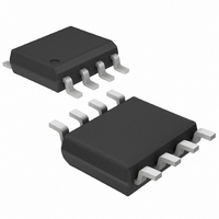
MAX1681ESA+T Maxim Integrated Products, MAX1681ESA+T Datasheet - Page 2

MAX1681ESA+T
Manufacturer Part Number
MAX1681ESA+T
Description
IC VOLT CONV 125MA 8-SOIC
Manufacturer
Maxim Integrated Products
Type
Switched Capacitor (Charge Pump), Doubler, Invertingr
Datasheet
1.MAX1680ESA.pdf
(12 pages)
Specifications of MAX1681ESA+T
Internal Switch(s)
Yes
Synchronous Rectifier
No
Number Of Outputs
1
Voltage - Output
-2 ~ -5.5 V, 4 ~ 11 V
Current - Output
125mA
Frequency - Switching
500kHz, 1MHz
Voltage - Input
2 ~ 5.5 V
Operating Temperature
-40°C ~ 85°C
Mounting Type
Surface Mount
Package / Case
8-SOIC (3.9mm Width)
Power - Output
471mW
Function
Inverting, Step Up
Output Voltage
- 3 V to - 5.5 V, 8 V to 11 V
Output Current
125 mA
Maximum Operating Temperature
+ 85 C
Minimum Operating Temperature
- 40 C
Mounting Style
SMD/SMT
Lead Free Status / RoHS Status
Lead free / RoHS Compliant
ABSOLUTE MAXIMUM RATINGS
IN ..............................................................................-0.3V to +6V
LV....................................................(V
CAP+ ...........................................................-0.3V to (V
SHDN, FSEL ......................................(V
OUT, CAP- ..................................................................-6V to 0.3V
Continuous Output Current ..............................................135mA
Output Short-Circuit Duration to GND (Note 1) ...................1sec
125mA, Frequency-Selectable,
Switched-Capacitor Voltage Converters
Note 1: Shorting OUT to IN may damage the device and should be avoided.
Stresses beyond those listed under “Absolute Maximum Ratings” may cause permanent damage to the device. These are stress ratings only, and functional
operation of the device at these or any other conditions beyond those indicated in the operational sections of the specifications is not implied. Exposure to
absolute maximum rating conditions for extended periods may affect device reliability.
ELECTRICAL CHARACTERISTICS
( Typical Operating Circuits (inverter configuration), FSEL = LV = GND, V
(MAX1681), T
2
Input Voltage Range
Supply Current
Output Voltage Under Load
(Note 2)
Output Resistance (Note 2)
Output Resistance to Ground
in Shutdown
Shutdown Current
Input Bias Current (SHDN)
Input Bias Current (FSEL)
Shutdown, FSEL Thresholds
Switching Frequency
_______________________________________________________________________________________
PARAMETER
A
= 0°C to +85°C, unless otherwise noted. Typical values are at T
R
SYMBOL
OUT(SHUT)
I+
V
I
R
I
SHDN
f
LOAD
FSEL
OUT
V
SHDN
V
OSC
V
OUT
I+
IN
IH
LV
IL
- 0.3V) to (V
- 0.3V) to (V
Inverter configuration,
R
Doubler configuration,
R
MAX1680
MAX1681
I
FSEL = IN or LV
SHDN = IN
OUT = GND, SHDN = IN
LV = GND (Note 3)
MAX1680
MAX1681
LOAD
L
L
= 1kΩ, LV = GND
= 1kΩ, LV = OUT
IN
IN
IN
= 125mA
+ 0.3V)
+ 0.3V)
+ 0.3V)
CONDITIONS
FSEL = IN
(125kHz)
FSEL = LV
(250kHz)
FSEL = IN
(500kHz)
FSEL = LV
(1MHz)
FSEL = LV
FSEL = IN
FSEL = LV
FSEL = IN
Continuous Power Dissipation (T
Operating Temperature Range ...........................-40°C to +85°C
Junction Temperature ......................................................+150°C
Storage Temperature Range .............................-65°C to +160°C
Lead Temperature (soldering, 10sec) .............................+300°C
SO (derate 5.88mW/°C above +70°C) ..........................471mW
IN
= 5V, C1 = C2 = 10µF (MAX1680), C1 = C2 = 2.2µF
A
= +25°C.)
T
T
T
T
T
T
T
T
MAX1680
MAX1681
MAX1680
MAX1681
A
A
A
A
A
A
A
A
= +25°C
= +25°C
= +25°C
= +25°C
= +25°C
= +25°C
= +25°C
= +25°C
-3.75
MIN
187
157
750
570
375
285
2.0
3.0
2.5
4.0
94
79
-1
-1
4
A
= +70°C)
-4.56
1000
TYP
250
125
500
2.5
3.5
10
20
5
1
MAX
1250
1490
10.8
21.6
43.2
313
348
156
174
625
745
5.5
5.5
5.5
5.5
4.5
5.4
18
36
10
9
5
1
1
1
1
UNITS
kHz
mA
µA
µA
µA
Ω
Ω
V
V
V
V


