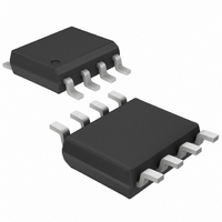
MAX861CSA+ Maxim Integrated Products, MAX861CSA+ Datasheet - Page 6

MAX861CSA+
Manufacturer Part Number
MAX861CSA+
Description
IC VOLT CONV SW-CAP 8-SOIC
Manufacturer
Maxim Integrated Products
Type
Switched Capacitor (Charge Pump), Doubler, Invertingr
Datasheet
1.MAX860ISA.pdf
(11 pages)
Specifications of MAX861CSA+
Internal Switch(s)
Yes
Synchronous Rectifier
No
Number Of Outputs
1
Voltage - Output
-1.5 ~ -5.5 V, 3 ~ 11 V
Current - Output
50mA
Frequency - Switching
13kHz, 100kHz, 250kHz
Voltage - Input
1.5 ~ 5.5 V
Operating Temperature
0°C ~ 70°C
Mounting Type
Surface Mount
Package / Case
8-SOIC (3.9mm Width)
Power - Output
471mW
Output Voltage
- 1.5 V to - 5.5 V, 5 V to 11 V
Output Current
100 mA
Maximum Power Dissipation
471 mW
Switching Frequency
250 KHz
Lead Free Status / RoHS Status
Lead free / RoHS Compliant
The MAX860/MAX861 capacitive charge pumps either
invert or double the voltage applied to their inputs. For
highest performance, use low equivalent series resis-
tance (ESR) capacitors. See the Capacitor Selection
section for more details. The frequency-control (FC) pin
allows you to choose one of three switching frequen-
cies; these three selectable frequencies are different for
each device. When shut down, MAX860/MAX861 cur-
rent consumption reduces to less than 1µA.
The most common application for these devices is a
charge-pump voltage inverter (see Typical Operating
Circuits). This application requires only two external com-
ponents—capacitors C1 and C2—plus a bypass capacitor
if necessary (see Bypass Capacitor section). Refer to the
Capacitor Selection section for suggested capacitor types
and values.
Even though the MAX860/MAX861’s output is not actively
regulated, it is fairly insensitive to load-current changes. A
circuit output source resistance of 12
the formula given in the Capacitor Selection section)
means that, with a +5V input, the output voltage is -5V
under no load and decreases to -4.4V with a 50mA load.
The MAX860/MAX861 output source resistance (used to
calculate the circuit output source resistance) vs. tempera-
ture and supply voltage are shown in the Typical
Operating Characteristics graphs.
Calculate the output ripple voltage using the formula
given in the Capacitor Selection section.
The MAX860/MAX861 can also operate as positive volt-
age doublers (see Typical Operating Circuits). This
application requires only two external components,
capacitors C1 and C2. The no-load output is twice the
input voltage. The electrical specifications in the doubler
mode are very similar to those of the inverter mode
except for the Supply Voltage Range (see Electrical
Characteristics table) and No-Load Supply Current (see
graph in Typical Operating Characteristics). The circuit
output source resistance and output ripple voltage are
calculated using the formulas in the Capacitor Selection
section.
When driven low, the
device. In inverter mode, connect
not used. In doubler mode, connect
50mA, Frequency-Selectable,
Switched-Capacitor Voltage Converters
6
_______________Detailed Description
_______________________________________________________________________________________
Active-Low Shutdown Input
S
–
—
H
—
Common Applications
D
—
N
Positive Voltage Doubler
–
input shuts down the
–
S
—
H
—
–
S
—
D
H
—
Voltage Inverter
(calculated using
—
N
–
D
—
N
–
to V
to GND if it
DD
if it is
is not used. When the device is shut down, all active
circuitry is turned off.
In the inverting configuration, loads connected from
OUT to GND are not powered in shutdown mode.
However, a reverse-current path exists through two
diodes between OUT and GND; therefore, loads con-
nected from V
supply.
In the doubling configuration, loads connected from the
V
mode. Loads connected from the V
pin draw current from the input supply through a path
similar to that of the inverting configuration (described
above).
Charge-pump frequency for both devices can be set to
one of three values. Each device has a unique set of
three available frequencies, as indicated in Table 1.
The oscillator and charge-pump frequencies are the
same (i.e., the charge-pump frequency is not half the
oscillator frequency, as it is on the MAX660, MAX665,
and ICL7660).
*See the Electrical Characteristics for detailed switching-
frequency specifications.
A higher switching frequency minimizes capacitor size
for the same performance and increases the supply
current (Table 2). The lowest fundamental frequency of
the switching noise is equal to the minimum specified
switching frequency (e.g., 3kHz for the MAX860 with FC
open). The spectrum of noise frequencies extends
above this value because of harmonics in the switching
waveform. To get best noise performance, choose the
device and FC connection to select a minimum switch-
ing frequency that lies above your sensitive bandwidth.
LV should be connected to GND for inverting operation.
To enhance compatibility with the MAX660, MAX665, and
ICL7660, you may float LV if the input voltage exceeds 3V.
In doubling mode, LV must be connected to OUT for all
input voltages.
Table 1. Nominal Switching Frequencies*
DD
FC = V
FC = GND
FC = OUT
pin to the GND pin are not powered in shutdown
FC CONNECTION
DD
or open
DD
to OUT draw current from the input
Low-Voltage-Operation Input
MAX860
Frequency Control
FREQUENCY (kHz)
130
50
6
DD
pin to the OUT
MAX861
100
250
13


