LM2596DSADJG ON Semiconductor, LM2596DSADJG Datasheet - Page 17
LM2596DSADJG
Manufacturer Part Number
LM2596DSADJG
Description
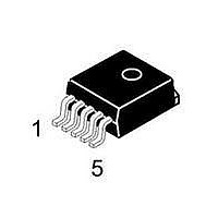
IC REG SW STP-DWN 3A D2PAK-5
Manufacturer
ON Semiconductor
Type
Step-Down (Buck)r
Datasheet
1.LM2596DSADJR4G.pdf
(25 pages)
Specifications of LM2596DSADJG
Internal Switch(s)
Yes
Synchronous Rectifier
No
Number Of Outputs
1
Voltage - Output
1.23 ~ 37 V
Current - Output
3A
Frequency - Switching
150kHz
Voltage - Input
4.5 ~ 40 V
Operating Temperature
-40°C ~ 125°C
Mounting Type
Surface Mount
Package / Case
D²Pak, TO-263 (5 leads + tab)
Output Voltage
1.23 V to 37 V
Output Current
3 A
Input Voltage
4.5 V to 40 V
Switching Frequency
150 KHz
Operating Temperature Range
- 40 C to + 125 C
Mounting Style
SMD/SMT
Duty Cycle (max)
95 %
Isolated/non-isolated
Non Isolated
Lead Free Status / RoHS Status
Lead free / RoHS Compliant
Power - Output
-
Lead Free Status / Rohs Status
Lead free / RoHS Compliant
Available stocks
Company
Part Number
Manufacturer
Quantity
Price
Company:

Part Number:
LM2596DSADJG
Manufacturer:
ON
Quantity:
12 400


heat
improvements are needed, double sided or multilayer PC
boards with large copper areas should be considered. In
order to achieve the best thermal performance, it is highly
recommended to use wide copper traces as well as large
areas of copper in the printed circuit board layout. The only
exception to this is the OUTPUT (switch) pin, which should
not have large areas of copper (see page 8 ‘PCB Layout
Guideline’).
Thermal Analysis and Design
whether or not a heatsink will be required. First determine:
1. P
2. T
3. T
4. R
5. R
(Refer to Maximum Ratings on page 2 of this data sheet or
R
total power dissipated by the LM2596:
where d is the duty cycle and for buck converter
I
V
Q
qJC
in
The following procedure must be performed to determine
The following formula is to calculate the approximate
D(max)
A(max
J(max)
qJC
qJA
and R
(quiescent current) and V
LM2596 data sheet,
is minimum input voltage applied,
dissipation
)
qJA
P
maximum regulator power dissipation in the
application.
maximum ambient temperature in the
application.
maximum allowed junction temperature
(125°C for the LM2596). For a conservative
design, the maximum junction temperature
should not exceed 110°C to assure safe
operation. For every additional +10°C
temperature rise that the junction must
withstand, the estimated operating lifetime
of the component is halved.
package thermal resistance junction−case.
package thermal resistance junction−ambient.
values).
D
= (V
significantly.
in
d +
x I
Unregulated
100 mF/50 V
12 to 40 V
Q
t on
DC Input
T
) + d x I
+
sat
C
V
V in
in
can be found in the
O
Load
Figure 22. Inverting Buck−Boost Develops −12 V
,
If
x V
+V
further
sat
in
LM2596−ADJ
ON/OFF
thermal
http://onsemi.com
GND
17
Feedback
V
I
turn−off can be neglected if proper type catch diode is used.
Packages Not on a Heatsink (Free−Standing)
the junction temperature can be determined by the following
expression:
where (R
caused by the dissipated power and T
ambient temperature.
Packages on a Heatsink
the selected safe operating junction temperature determined
in step 3, than a heatsink is required. The junction
temperature will be calculated as follows:
where
selected safe operating junction temperature, then a larger
heatsink is required.
Some Aspects That can Influence Thermal Design
the junction temperature rise numbers are all approximate,
and there are many factors that will affect these numbers,
such as PC board size, shape, thickness, physical position,
location, board temperature, as well as whether the
surrounding air is moving or still.
area, copper thickness, single− or double−sided, multilayer
board, the amount of solder on the board or even color of the
traces.
board can also influence its effectiveness to dissipate the heat.
Load
O
The dynamic switching losses during turn−on and
For a free−standing application when no heatsink is used,
If the actual operating junction temperature is greater than
If the actual operating temperature is greater than the
It should be noted that the package thermal resistance and
Other factors are trace width, total printed circuit copper
The size, quantity and spacing of other components on the
D1
1N5822
33 mH
is the regulator output voltage,
is the load current.
L1
R
R
R
qJA
qJC
qCS
qSA
T
)(P
J
C
220 mF
is the thermal resistance junction−case,
= P
is the thermal resistance case−heatsink,
is the thermal resistance heatsink−ambient.
D
out
) represents the junction temperature rise
D
T
J
(R
= (R
qJA
R3
qJA
+ R
R4
−12 V @ 0.7 A
Regulated
) (P
qCS
Output
D
+ R
) + T
qSA
A
A
) + T
is the maximum
A
Related parts for LM2596DSADJG
Image
Part Number
Description
Manufacturer
Datasheet
Request
R

Part Number:
Description:
ON Semiconductor [VOLTAGE REGULATOR]
Manufacturer:
ON Semiconductor
Datasheet:
Part Number:
Description:
357-036-542-201 CARDEDGE 36POS DL .156 BLK LOPRO
Manufacturer:
ON Semiconductor
Datasheet:
Part Number:
Description:
357-036-542-201 CARDEDGE 36POS DL .156 BLK LOPRO
Manufacturer:
ON Semiconductor
Datasheet:
Part Number:
Description:
357-036-542-201 CARDEDGE 36POS DL .156 BLK LOPRO
Manufacturer:
ON Semiconductor
Datasheet:
Part Number:
Description:
357-036-542-201 CARDEDGE 36POS DL .156 BLK LOPRO
Manufacturer:
ON Semiconductor
Datasheet:
Part Number:
Description:
357-036-542-201 CARDEDGE 36POS DL .156 BLK LOPRO
Manufacturer:
ON Semiconductor
Datasheet:
Part Number:
Description:
357-036-542-201 CARDEDGE 36POS DL .156 BLK LOPRO
Manufacturer:
ON Semiconductor
Datasheet:
Part Number:
Description:
357-036-542-201 CARDEDGE 36POS DL .156 BLK LOPRO
Manufacturer:
ON Semiconductor
Datasheet:
Part Number:
Description:
357-036-542-201 CARDEDGE 36POS DL .156 BLK LOPRO
Manufacturer:
ON Semiconductor
Datasheet:
Part Number:
Description:
357-036-542-201 CARDEDGE 36POS DL .156 BLK LOPRO
Manufacturer:
ON Semiconductor
Datasheet:
Part Number:
Description:
357-036-542-201 CARDEDGE 36POS DL .156 BLK LOPRO
Manufacturer:
ON Semiconductor
Datasheet:
Part Number:
Description:
Manufacturer:
ON Semiconductor
Datasheet:
Part Number:
Description:
Manufacturer:
ON Semiconductor
Datasheet:
Part Number:
Description:
Manufacturer:
ON Semiconductor
Datasheet: