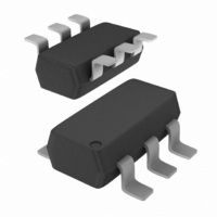
MAX1720EUTG ON Semiconductor, MAX1720EUTG Datasheet - Page 13

MAX1720EUTG
Manufacturer Part Number
MAX1720EUTG
Description
IC INVERTER CHRG PUMP VOLT 6TSOP
Manufacturer
ON Semiconductor
Type
Switched Capacitor (Charge Pump), Invertingr
Datasheet
1.MAX1720EUTG.pdf
(18 pages)
Specifications of MAX1720EUTG
Internal Switch(s)
Yes
Synchronous Rectifier
No
Number Of Outputs
1
Voltage - Output
-1.5 ~ -5.5 V, 3 ~ 11 V
Current - Output
50mA
Frequency - Switching
12kHz
Voltage - Input
1.5 ~ 5.5 V
Operating Temperature
-40°C ~ 85°C
Mounting Type
Surface Mount
Package / Case
SC-74-6
Power - Output
313mW
Function
Inverting
Output Voltage
- 5.5 V to - 1.15 V
Output Current
100 mA
Maximum Operating Temperature
+ 150 C
Mounting Style
SMD/SMT
Operating Supply Voltage (min)
1.15V
Operating Supply Voltage (max)
5.5V
Package Type
TSOP
Pin Count
6
Mounting
Surface Mount
Lead Free Status / RoHS Status
Lead free / RoHS Compliant
Other names
MAX1720EUTGOS
Available stocks
Company
Part Number
Manufacturer
Quantity
Price
Company:
Part Number:
MAX1720EUTG
Manufacturer:
ON Semiconductor
Quantity:
1 150
devices. The output current capability is approximately equal to the number of devices paralleled. A single shared output capacitor
is sufficient for proper operation but each device does require it’s own pump capacitor. Note that the output ripple frequency will
be complex since the oscillators are not synchronized. The performance characteristics for a converter consisting of two paralleled
devices is shown below.
transistors and two Schottky diodes. The output voltage is approximately equal to −V
both transistors and the forward voltage of both diodes. The performance characteristics for the converter are shown below. Note
that the output resistance is reduced to 0.9 W.
An increase in converter output current capability with a reduction in output resistance can be obtained by paralleling two or more
The output current capability of the MAX1720 can be extended beyond 600 mA with the addition of two external switch
Curve
A
B
V
in
Figure 37. External Switch for Increased Negative Output Current
V
in
5.0
3.0
+
(V)
−V
C
out
3
Figure 38. Current Boosted Load Regulation, Output Voltage vs. Output Current
= V
R
out
14.5
1
2
3
17
in
(W)
−V
BE(Q1) −
OSC
−2.2
−2.4
−2.6
−2.8
−3.0
−3.2
V
http://onsemi.com
BE(Q2)
0
MAX1720
6
5
4
−2 V
13
0.1
F
−1.0
−2.0
−3.0
−4.0
−5.0
0
I
out
0
Q
Q
, OUTPUT CURRENT (mA)
2
1
0.2
Figure 36. Parallel Load Regulation, Output
C
C
Q
Q
T
+
A
10
1
3
1
2
C
= C
= 220 mF
= 25°C
= PZT751
= PZT651
1
2
20
= 470 mF
0.3
Voltage vs. Output Current
in
I
out
minus the sum of the base emitter drops of
30
+
, OUTPUT CURRENT (mA)
0.4
40
C
B
2
−V
V
R
T
50
A
in
A
out
out
= 25°C
= 5.0 V
= 0.9 W
0.5
60
70
0.6
80
90
100


