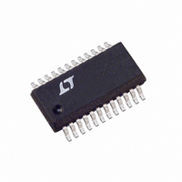
LTC1436AIGN-PLL#TR Linear Technology, LTC1436AIGN-PLL#TR Datasheet - Page 11

LTC1436AIGN-PLL#TR
Manufacturer Part Number
LTC1436AIGN-PLL#TR
Description
IC REG SW SYNC STEPDWN LN 24SSOP
Manufacturer
Linear Technology
Type
Step-Down (Buck)r
Datasheet
1.LTC1436AIGN-PLLPBF.pdf
(28 pages)
Specifications of LTC1436AIGN-PLL#TR
Internal Switch(s)
No
Synchronous Rectifier
Yes
Number Of Outputs
1
Voltage - Output
1.19 ~ 9 V
Current - Output
50mA
Frequency - Switching
125kHz ~ 240kHz
Voltage - Input
3.5 ~ 30 V
Operating Temperature
-40°C ~ 85°C
Mounting Type
Surface Mount
Package / Case
24-SSOP
Lead Free Status / RoHS Status
Contains lead / RoHS non-compliant
Power - Output
-
Other names
LTC1436AIGN-PLLTR
Available stocks
Company
Part Number
Manufacturer
Quantity
Price
Part Number:
LTC1436AIGN-PLL#TRLTC1436AIGN-PLL
Manufacturer:
Linear Technology
Quantity:
135
OPERATIO
APPLICATIONS
Power-On Reset
The POR pin is an open drain output which pulls low when
the main regulator output voltage is out of regulation.
When the output voltage rises to within 7.5% of regula-
tion, a timer is started which releases POR after 2
(65536) oscillator cycles. In shutdown, the POR output is
pulled low.
Auxiliary Linear Regulator
The auxiliary linear regulator in the LTC1436A/LTC1437A
controls an external PNP transistor for operation up to
500mA. An internal AUXFB resistive divider set for 12V
operation is invoked when AUXDR pin is above 9.5V to
allow 12V VPP supplies to be easily implemented. When
AUXDR is below 8.5V an external feedback divider may be
used to set other output voltages. Taking the AUXON pin
low shuts down the auxiliary regulator providing a conve-
nient logic controlled power supply.
The basic LTC1436A application circuit is shown in Figure
1, High Efficiency Step-Down Converter. External compo-
nent selection is driven by the load requirement, and
begins with the selection of R
known, C
MOSFETs and D1 are selected. Finally, C
selected. The circuit shown in Figure 1 can be configured
for operation up to an input voltage of 28V (limited by the
external MOSFETs).
R
R
The LTC1436A/LTC1437A current comparator has a maxi-
mum threshold of 150mV/R
mode range of SGND to INTV
threshold sets the peak of the inductor current, yielding a
maximum average output current I
value less half the peak-to-peak ripple current ∆I
Allowing a margin for variations in the LTC1436A/
LTC1437A and external component values yields:
SENSE
SENSE
Selection For Output Current
is chosen based on the required output current.
OSC
and L can be chosen. Next, the power
U
U
(Refer to Functional Diagram)
INFORMATION
U
SENSE
CC
. The current comparator
SENSE
and an input common
MAX
W
. Once R
equal to the peak
IN
and C
U
SENSE
L
OUT
.
are
16
is
The AUX block can be used as a comparator having its
inverting input tied to the internal 1.19V reference. The
AUXDR pin is used as the output and requires an external
pull-up to a supply less than 8.5V in order to inhibit the
invoking of the internal resistive divider.
INTV
Power for the top and bottom MOSFET drivers and most
of the other LTC1436A/LTC1437A circuitry is derived from
the INTV
pin is internally connected to INTV
externally connected to INTV
the EXTV
regulator supplies INTV
4.8V, the 5V regulator is turned off and an internal switch
is turned on to connect EXTV
INTV
source such as the output of the regulator itself or a
secondary winding, as described in the Applications Infor-
mation section.
The LTC1436A/LTC1437A work well with R
≥ 0.005Ω.
C
The LTC1436A/LTC1437A use a constant frequency
architecture with the frequency determined by an external
oscillator capacitor C
turns on, the voltage on C
on-time, C
additional current which is proportional to the output
voltage of the phase detector V
LTC1437A). When the voltage on the capacitor reaches
1.19V, C
The value of C
frequency. Assuming the phase-locked loop has no exter-
nal oscillator input (V
OSC
R
SENSE
CC
CC
Selection for Operating Frequency
/DRV
power to be derived from a high efficiency external
OSC
CC
CC
=
OSC
pin. The bottom MOSFET driver supply DRV
LTC1436A-PLL/LTC1437A
pin is left open, an internal 5V low dropout
is reset to ground. The process then repeats.
CC
100
OSC
I
MAX
/EXTV
is charged by a fixed current plus an
mV
is calculated from the desired operating
OSC
PLLLPF
CC
CC
OSC
Power
. Each time the topside MOSFET
power. If EXTV
CC
is reset to ground. During the
= 0V):
CC
to INTV
in the LTC1437A. When
PLLLPF
CC
in the LTC1436A and
CC
LTC1436A
(LTC1436A-PLL/
CC
. This allows the
is taken above
SENSE
11
values
14367afb
CC


