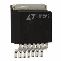
LT1374IR Linear Technology, LT1374IR Datasheet - Page 6

LT1374IR
Manufacturer Part Number
LT1374IR
Description
IC SW REG 4.5A ADJ STEP-DWN 7-DD
Manufacturer
Linear Technology
Type
Step-Down (Buck)r
Datasheet
1.LT1374CFEPBF.pdf
(32 pages)
Specifications of LT1374IR
Internal Switch(s)
Yes
Synchronous Rectifier
No
Number Of Outputs
1
Voltage - Output
2.42 ~ 21.5 V
Current - Output
4.5A
Frequency - Switching
500kHz
Voltage - Input
5 ~ 25 V
Operating Temperature
-40°C ~ 125°C
Mounting Type
Surface Mount
Package / Case
D²Pak, TO-263 (7 leads + tab)
Lead Free Status / RoHS Status
Contains lead / RoHS non-compliant
Power - Output
-
Available stocks
Company
Part Number
Manufacturer
Quantity
Price
Part Number:
LT1374IR
Manufacturer:
LT
Quantity:
20 000
Part Number:
LT1374IR#PBF
Manufacturer:
LINEAR/凌特
Quantity:
20 000
Part Number:
LT1374IR#TRPBF
Manufacturer:
LINEAR/凌特
Quantity:
20 000
Part Number:
LT1374IR-5SYNC#PBF
Manufacturer:
LINEAR/凌特
Quantity:
20 000
Part Number:
LT1374IR-SYNC#PBF
Manufacturer:
LINEAR/凌特
Quantity:
20 000
LT1374
TYPICAL PERFOR A CE CHARACTERISTICS
PI FU CTIO S
FB/SENSE: The feedback pin is the input to the error
amplifier which is referenced to an internal 2.42V source.
An external resistive divider is used to set the output
voltage. The fixed voltage (-5) parts have the divider
included on-chip and the FB pin is used as a SENSE pin,
connected directly to the 5V output. Three additional
functions are performed by the FB pin. When the pin
voltage drops below 1.7V, switch current limit is reduced.
Below 1.5V the external sync function is disabled. Below
1V, switching frequency is also reduced. See Feedback Pin
Function section in Applications Information for details.
BOOST: The BOOST pin is used to provide a drive voltage,
higher than the input voltage, to the internal bipolar NPN
power switch. Without this added voltage, the typical
switch voltage loss would be about 1.5V. The additional
boost voltage allows the switch to saturate and voltage
loss approximates that of a 0.07Ω FET structure. Effi-
ciency improves from 75% for conventional bipolar de-
signs to > 89% for these new parts.
V
This pin powers the internal circuitry and internal regulator
when the BIAS pin is not present. At NPN switch on and off,
high dI/dt edges occur on this pin. Keep the external
bypass and catch diode close to this pin. All trace induc-
tance on this path will create a voltage spike at switch off,
adding to the V
6
IN
100
40
30
90
80
70
60
50
10
U
20
: This is the collector of the on-chip power NPN switch.
0
0
BOOST Pin Current
DUTY CYCLE = 100%
U
1
SWITCH CURRENT (A)
CE
2
voltage across the internal NPN. Both V
U
3
W
4
1374 G16
U
5
1.4
1.2
1.0
0.8
0.6
0.4
–50
V
C
SHUTDOWN
Pin Shutdown Threshold
–25
JUNCTION TEMPERATURE (°C)
0
IN
25
50
pins of the 16-lead TSSOP package must be shorted
together on the PC board.
GND: The GND pin connection needs consideration for
two reasons. First, it acts as the reference for the regulated
output, so load regulation will suffer if the “ground” end of
the load is not at the same voltage as the GND pin of the
IC. This condition will occur when load current or other
currents flow through metal paths between the GND pin
and the load ground point. Keep the ground path short
between the GND pin and the load and use a ground plane
when possible. The second consideration is EMI caused
by GND pin current spikes. Internal capacitance between
the V
current spikes in the GND pin. If the GND pin is connected
to system ground with a long metal trace, this trace may
radiate excess EMI. Keep the path between the input
bypass and the GND pin short.
V
NPN switch. This pin is driven up to the input pin voltage
during switch on time. Inductor current drives the switch
pin negative during switch off time. Negative voltage is
clamped with the external catch diode. Maximum negative
switch voltage allowed is – 0.8V. Both V
16-lead TSSOP package must be shorted together on the
PC board.
SW
75
: The switch pin is the emitter of the on-chip power
SW
100
pin and the GND pin creates very narrow (<10ns)
1374 G11
125
0.001
0.01
1.0
0.1
0
Inductor Core Loss
CORE LOSS IS
INDEPENDENT OF LOAD
CURRENT UNTIL LOAD CURRENT FALLS
LOW ENOUGH FOR CIRCUIT TO GO INTO
DISCONTINUOUS MODE
V
OUT
= 5V, V
5
INDUCTANCE (µH)
IN
10
= 10V, I
OUT
TYPE 52
POWDERED IRON
Kool Mµ
PERMALLOY
µ = 125
15
= 1A
SW
®
20
pins of the
1374 G01
25
20
12
8
4
2
1.2
0.8
0.4
0.2
0.12
0.08
0.04
0.02
1374fd


