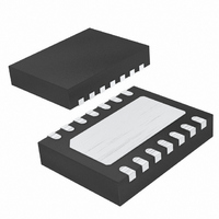
LT3980EDE#TRPBF Linear Technology, LT3980EDE#TRPBF Datasheet - Page 15

LT3980EDE#TRPBF
Manufacturer Part Number
LT3980EDE#TRPBF
Description
IC SWITCHING REG STP-DN 2A 14DFN
Manufacturer
Linear Technology
Type
Step-Down (Buck)r
Datasheet
1.LT3980EDETRPBF.pdf
(24 pages)
Specifications of LT3980EDE#TRPBF
Internal Switch(s)
Yes
Synchronous Rectifier
No
Number Of Outputs
1
Voltage - Output
0.79 ~ 52.2 V
Current - Output
2A
Frequency - Switching
100kHz ~ 2.4MHz
Voltage - Input
3.6 ~ 58 V
Operating Temperature
-40°C ~ 125°C
Mounting Type
Surface Mount
Package / Case
14-DFN
Lead Free Status / RoHS Status
Lead free / RoHS Compliant
Power - Output
-
Available stocks
Company
Part Number
Manufacturer
Quantity
Price
APPLICATIONS INFORMATION
While operating with high boost voltages (>10V), it is
important to ensure that the power dissipation from the
boost circuit is not too high. See the Typical Performance
Characteristics section for the plot, BOOST Pin Current
vs Switch Current. Boost circuit power dissipation is
calculated as follows:
Where DC is the switch duty cycle, I
current, and V
pin and switch pin. If the P
between the boost pin and the boost capacitor such that the
power is dissipated in the Zener instead of the LT3980.
The minimum operating voltage of an LT3980 application
is limited by the minimum input voltage (3.6V) and by the
maximum duty cycle as outlined in a previous section. For
proper startup, the minimum input voltage is also limited
by the boost circuit. If the input voltage is ramped slowly,
or the LT3980 is turned on with its RUN/SS pin when the
output is already in regulation, then the boost capacitor
may not be fully charged. Because the boost capacitor is
charged with the energy stored in the inductor, the circuit
will rely on some minimum load current to get the boost
circuit running properly. This minimum load will depend
P
BOOST
= I
BOOST
BOOST
Figure 6. The Minimum Input Voltage Depends on Output Voltage, Load Current and Boost Circuit
6
5
4
3
2
1
V
– V
BOOST
TO START
TO RUN
SW
BOOST
is the voltage between the boost
– SW
10
I
LOAD
> 0.5W, a Zener can be put
DC
(mA)
BOOST
100
f = 400kHz
V
is the boost pin
OUT
= 3.3V
1000 2000
3980 F06a
on input and output voltages, and on the arrangement of
the boost circuit. The minimum load generally goes to
zero once the circuit has started. Figure 6 shows a plot
of minimum load to start and to run as a function of input
voltage. In many cases the discharged output capacitor
will present a load to the switcher, which will allow it to
start. The plots show the worst-case situation where V
is ramping very slowly. For lower start-up voltage, the
boost diode can be tied to V
input range to one-half of the absolute maximum rating
of the BOOST pin.
At light loads, the inductor current becomes discontinu-
ous and the effective duty cycle can be very high. This
reduces the minimum input voltage to approximately
300mV above V
current is continuous and the duty cycle is limited by the
maximum duty cycle of the LT3980, requiring a higher
input voltage to maintain regulation.
Soft-Start
The RUN/SS pin can be used to soft-start the LT3980,
reducing the maximum input current during start-up.
The RUN/SS pin is driven through an external RC fi lter to
8
7
6
5
4
1
TO START
TO RUN
OUT
10
. At higher load currents, the inductor
I
LOAD
(mA)
100
IN
; however, this restricts the
f = 400kHz
V
OUT
1000 2000
= 5V
3980 F06b
LT3980
15
3980f
IN


