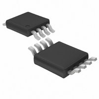
LTC1474CMS8 Linear Technology, LTC1474CMS8 Datasheet - Page 13

LTC1474CMS8
Manufacturer Part Number
LTC1474CMS8
Description
IC CONV STEP-DWN HI-EFF 8-MSOP
Manufacturer
Linear Technology
Type
Step-Down (Buck)r
Datasheet
1.LTC1474CS8-5PBF.pdf
(20 pages)
Specifications of LTC1474CMS8
Internal Switch(s)
Yes
Synchronous Rectifier
No
Number Of Outputs
1
Voltage - Output
Adjustable
Current - Output
750mA
Voltage - Input
3 ~ 18 V
Operating Temperature
0°C ~ 70°C
Mounting Type
Surface Mount
Package / Case
8-MSOP, Micro8™, 8-uMAX, 8-uSOP,
Lead Free Status / RoHS Status
Contains lead / RoHS non-compliant
Power - Output
-
Frequency - Switching
-
Available stocks
Company
Part Number
Manufacturer
Quantity
Price
Company:
Part Number:
LTC1474CMS8
Manufacturer:
LT
Quantity:
5 321
Company:
Part Number:
LTC1474CMS8
Manufacturer:
LT
Quantity:
10 000
Part Number:
LTC1474CMS8
Manufacturer:
LT
Quantity:
20 000
Company:
Part Number:
LTC1474CMS8#TRPBF
Manufacturer:
LINEAR
Quantity:
7 938
Part Number:
LTC1474CMS8#TRPBF
Manufacturer:
LINEAR/凌特
Quantity:
20 000
Company:
Part Number:
LTC1474CMS8-3.3
Manufacturer:
LT
Quantity:
10 000
Part Number:
LTC1474CMS8-3.3
Manufacturer:
LT/凌特
Quantity:
20 000
Company:
Part Number:
LTC1474CMS8-5
Manufacturer:
LT
Quantity:
10 000
APPLICATIONS
5. Are the signal and power grounds segregated? The
6. Is a 100k resistor connected in series between RUN
Design Example (Refer to R
Selection)
As a design example, assume V
a maximum average output current I
this information, we can easily calculate all the important
components:
From the equation (1),
Using the standard resistors (1 , 1 and 2 ) in parallel
provides 0.4 without having to use a more expensive
low value current shunt type resistor (see R
tion section).
With R
calculated from (2), neglecting the second term, to be
signal ground consists of the (–) plate of C
the LTC1474/LTC1475 and the resistive divider. The
power ground consists of the Schottky diode anode,
the (–) plate of C
(Pin 8) and the RUN control voltage? The resistor
should be as close as possible to Pin 8.
R
SENSE
SENSE
= (0.067/0.1) – 0.25 = 0.42
= 0.4 , the peak inductor current I
IN
U
and the 0.1 F decoupling capacitor.
INFORMATION
U
Figure 9. LTC1474/LTC1475 Layout Diagram (See Board Layout Checklist)
SENSE
V
OUT
IN
= 10V, V
+
and Inductor
W
BOLD LINES INDICATE HIGH PATH CURRENTS
MAX
C
OUT
= 100mA. With
R2
OUT
SENSE
OUT
R1
10pF
= 3V, and
U
, Pin 4 of
PEAK
Selec-
0.1 F
C
IN
1
2
3
4
+
OUTPUT DIVIDER REQUIRED WITH
ADJUSTABLE VERSION ONLY
is
V
LBO
LBI
GND
FB
LTC1474
150mA. The minimum inductance is, therefore, from the
equation (3) and assuming V
From Figure 3, an inductance of 270 H is chosen from the
recommended region. The CDRH73-271 or CD54-271 is a
good choice for space limited applications.
For the feedback resistors, choose R1 = 1M to minimize
supply current. R2 can then be calculated from the equa-
tion (4) to be:
For the catch diode, the MBR0530 will work well in this
application.
For the input and output capacitors, AVX 4.7 F and 100 F,
respectively, low ESR TPS series work well and meet the
RMS current requirement of 100mA/2 = 50mA. They are
available in small “C” case sizes with 0.15
0.15 output capacitor ESR will result in 25mV of output
voltage ripple.
Figure 10 shows the complete circuit for this example.
SENSE
RUN
L
R
D1
SW
V
IN
MIN
2
8
7
6
5
V
IN
100k
V
1 23
0 75 3 3 0 4 4 75
OUT
.
1000pF
1
0 15 0 1
R
SENSE
1474/75 F09
R
1 1 43
LTC1474/LTC1475
L
.
D
= 0.4V,
M
s
264
H
ESR. The
13


