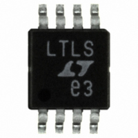
LT1767EMS8-1.8#TR Linear Technology, LT1767EMS8-1.8#TR Datasheet - Page 14

LT1767EMS8-1.8#TR
Manufacturer Part Number
LT1767EMS8-1.8#TR
Description
IC SW REG STEP-DOWN 1.8V 8-MSOP
Manufacturer
Linear Technology
Type
Step-Down (Buck)r
Datasheet
1.LT1767EMS8-3.3PBF.pdf
(16 pages)
Specifications of LT1767EMS8-1.8#TR
Internal Switch(s)
Yes
Synchronous Rectifier
No
Number Of Outputs
1
Voltage - Output
1.8V
Current - Output
1.5A
Frequency - Switching
1.25MHz
Voltage - Input
3 ~ 25 V
Operating Temperature
-40°C ~ 125°C
Mounting Type
Surface Mount
Package / Case
8-MSOP, Micro8™, 8-uMAX, 8-uSOP,
Lead Free Status / RoHS Status
Contains lead / RoHS non-compliant
Power - Output
-
Other names
LT1767EMS8-1.8TR
LT1767EMS81.8TR
LT1767EMS81.8TR
Available stocks
Company
Part Number
Manufacturer
Quantity
Price
LT1767/LT1767-1.8/
LT1767-2.5/LT1767-3.3/LT1767-5
APPLICATIONS
The zero produced by the ESR of the tantalum output
capacitor is very useful in maintaining stability. Ceramic
output capacitors do not have a zero due to very low ESR,
but are dominated by their ESL. They form a notch in the
1MHz to 10MHz range. Without this zero, the V
be made dominant. A typical value of 2.2nF will achieve
this.
If better transient response is required, a zero can be
added to the loop using a resistor (R
compensation capacitor. As the value of R
transient response will generally improve, but two effects
limit its value. First, the combination of output capacitor
ESR and a large R
gether. Second, if the loop gain is not rolled sufficiently at
the switching frequency, output ripple will perturb the V
pin enough to cause unstable duty cycle switching similar
to subharmonic oscillation. This may not be apparent at
the output. Small signal analysis will not show this since
a continuous time system is assumed. If needed, an
additional capacitor (C
typically one fifth the switching frequency (If R
C
When checking loop stability, the circuit should be oper-
ated over the application’s full voltage, current and tem-
perature range. Any transient loads should be applied and
the output voltage monitored for a well-damped behavior.
See Application Note 76 for more details.
CONVERTER WITH BACKUP OUTPUT REGULATOR
In systems with a primary and backup supply, for ex-
ample, a battery powered device with a wall adapter input,
the output of the LT1767 can be held up by the backup
supply with its input disconnected. In this condition, the
SW pin will source current into the V
is held at ground, only the shut down current of 6 A will
be pulled via the SW pin from the second supply. With the
SHDN pin floating, the LT1767 will consume its quiescent
operating current of 1mA. The V
current to any other components connected to the input
line. If this load is greater than 10mA or the input could be
shorted to ground, a series Schottky diode must be added,
as shown in Figure 9. With these safeguards, the output
can be held at voltages up to the V
rating.
14
F
= ~ 100pF).
C
U
may stop loop gain rolling off alto-
F
) can be added to form a pole at
INFORMATION
U
IN
IN
W
IN
pin will also source
C
absolute maximum
pin. If the SHDN pin
) in series with the
C
is increased,
C
U
pole must
C
= ~ 5k,
C
BUCK CONVERTER WITH ADJUSTABLE SOFT-START
Large capacitive loads or high input voltages can cause
high input currents at start-up. Figure 10 shows a circuit
that limits the dv/dt of the output at start-up, controlling
the capacitor charge rate. The buck converter is a typical
configuration with the addition of R3, R4, C
the output starts to rise, Q1 turns on, regulating switch
current via the V
output. Output rise time is controlled by the current
through C
is in regulation, Q1 turns off and the circuit operates
normally. R3 is transient protection for the base of Q1.
Using the values shown in Figure 10,
The ramp is linear and rise times in the order of 100ms are
possible. Since the circuit is voltage controlled, the ramp
rate is unaffected by load characteristics and maximum
output current is unchanged. Variants of this circuit can be
used for sequencing multiple regulator outputs.
Dual Output SEPIC Converter
The circuit in Figure 11 generates both positive and
negative 5V outputs with a single piece of magnetics. The
two inductors shown are actually just two windings on a
standard B H Electronics inductor. The topology for the 5V
output is a standard buck converter. The – 5V topology
would be a simple flyback winding coupled to the buck
converter if C4 were not present. C4 creates a SEPIC
(single-ended primary inductance converter) topology
which improves regulation and reduces ripple current in
L1. Without C4, the voltage swing on L1B compared to
L1A would vary due to relative loading and coupling
losses. C4 provides a low impedance path to maintain an
equal voltage swing in L1B, improving regulation. In a
flyback converter, during switch on time, all the converter’s
energy is stored in L1A only, since no current flows in L1B.
At switch off, energy is transferred by magnetic coupling
into L1B, powering the – 5V rail. C4 pulls L1B positive
RiseTime
RiseTime
SS
defined by R4 and Q1’s V
( )(
(
R C
C
47 10 15 10
4
pin to maintain a constant dv/dt at the
•
(
SS
V
3
BE
)( •
)(
0 7
)
V
.
OUT
)
–
9
)( )
5
BE
. Once the output
5
SS
ms
and Q1. As
sn1767 1767fas


