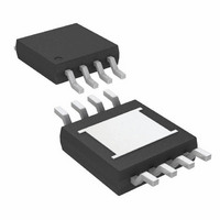
LT1961EMS8E Linear Technology, LT1961EMS8E Datasheet - Page 10

LT1961EMS8E
Manufacturer Part Number
LT1961EMS8E
Description
IC REG SW STEPUP 1.5A 8-MSOP
Manufacturer
Linear Technology
Type
Step-Up (Boost)r
Datasheet
1.LT1961EMS8E.pdf
(16 pages)
Specifications of LT1961EMS8E
Internal Switch(s)
Yes
Synchronous Rectifier
No
Number Of Outputs
1
Voltage - Output
1.2 ~ 35 V
Current - Output
1.5A
Frequency - Switching
1.25MHz
Voltage - Input
3 ~ 25 V
Operating Temperature
-40°C ~ 125°C
Mounting Type
Surface Mount
Package / Case
8-MSOP Exposed Pad, 8-HMSOP, 8-eMSOP
Lead Free Status / RoHS Status
Contains lead / RoHS non-compliant
Power - Output
-
Available stocks
Company
Part Number
Manufacturer
Quantity
Price
Company:
Part Number:
LT1961EMS8E
Manufacturer:
LINEAR
Quantity:
31
Part Number:
LT1961EMS8E
Manufacturer:
LINEAR/凌特
Quantity:
20 000
Part Number:
LT1961EMS8E#PBF
Manufacturer:
LINEAR/凌特
Quantity:
20 000
Company:
Part Number:
LT1961EMS8E#TRPBF
Manufacturer:
AMIS
Quantity:
6 218
Part Number:
LT1961EMS8E#TRPBF
Manufacturer:
LINEAR/凌特
Quantity:
20 000
LT1961
APPLICATIONS
SYNCHRONIZATION
The SYNC pin, is used to synchronize the internal oscilla-
tor to an external signal. The SYNC input must pass from
a logic level low, through the maximum synchronization
threshold with a duty cycle between 20% and 80%. The
input can be driven directly from a logic level output. The
synchronizing range is equal to initial operating frequency
up to 2MHz. This means that minimum practical sync
frequency is equal to the worst-case high self-oscillating
frequency (1.5MHz), not the typical operating frequency
of 1.25MHz. Caution should be used when synchronizing
above 1.7MHz because at higher sync frequencies the
amplitude of the internal slope compensation used to
prevent subharmonic switching is reduced. Higher induc-
tor values will tend to eliminate this problem. See Fre-
quency Compensation section for a discussion of an
entirely different cause of subharmonic switching before
assuming that the cause is insufficient slope compensa-
tion. Application Note 19 has more details on the theory
of slope compensation.
LAYOUT CONSIDERATIONS
As with all high frequency switchers, when considering
layout, care must be taken to achieve optimal electrical,
thermal and noise performance. For maximum efficiency,
switch rise and fall times are typically in the nanosecond
range. To prevent noise both radiated and conducted, the
10
U
INFORMATION
U
V
W
IN
Figure 5. High Speed Switching Path
C3
LT1961
U
GND
SW
L1
FREQUENCY
SWITCHING
PATH
HIGH
high speed switching current path, shown in Figure 5,
must be kept as short as possible. This is implemented in
the suggested layout of Figure 6. Shortening this path will
also reduce the parasitic trace inductance of approxi-
mately 25nH/inch. At switch off, this parasitic inductance
produces a flyback spike across the LT1961 switch. When
operating at higher currents and output voltages, with
poor layout, this spike can generate voltages across the
LT1961 that may exceed its absolute maximum rating. A
ground plane should always be used under the switcher
circuitry to prevent interplane coupling and overall noise.
The V
possible from the switch node. The LT1961 pinout has
been designed to aid in this. The ground for these compo-
nents should be separated from the switch current path.
Failure to do so will result in poor stability or subharmonic
like oscillation.
Board layout also has a significant effect on thermal
resistance. The exposed pad is the copper plate that runs
under the LT1961 die. This is the best thermal path for heat
out of the package. Soldering the pad onto the board will
reduce die temperature and increase the power capability
of the LT1961. Provide as much copper area as possible
around this pad. Adding multiple solder filled feedthroughs
under and around the pad to the ground plane will also
help. Similar treatment to the catch diode and inductor
terminations will reduce any additional heating effects.
D1
C
and FB components should be kept as far away as
C1
LOAD
1961 F05
V
OUT
1961fa


