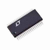
LTC1709EG-7 Linear Technology, LTC1709EG-7 Datasheet - Page 25

LTC1709EG-7
Manufacturer Part Number
LTC1709EG-7
Description
IC SW REG STEP-DOWN SYNC 36-SSOP
Manufacturer
Linear Technology
Type
Step-Down (Buck)r
Datasheet
1.LTC1709EG-7.pdf
(28 pages)
Specifications of LTC1709EG-7
Internal Switch(s)
No
Synchronous Rectifier
Yes
Number Of Outputs
2
Voltage - Output
1.3 ~ 3.5 V
Current - Output
3A
Voltage - Input
4 ~ 36 V
Operating Temperature
-40°C ~ 85°C
Mounting Type
Surface Mount
Package / Case
36-SSOP
Lead Free Status / RoHS Status
Contains lead / RoHS non-compliant
Power - Output
-
Frequency - Switching
-
Available stocks
Company
Part Number
Manufacturer
Quantity
Price
Company:
Part Number:
LTC1709EG-7
Manufacturer:
LT
Quantity:
392
Part Number:
LTC1709EG-7
Manufacturer:
LT/凌特
Quantity:
20 000
Company:
Part Number:
LTC1709EG-7#PBF
Manufacturer:
Linear Technology
Quantity:
135
APPLICATIO S I FOR ATIO
PC Board Layout Checklist
When laying out the printed circuit board, the following
checklist should be used to ensure proper operation of the
LTC1709-7. These items are also illustrated graphically in
the layout diagram of Figure 12. Check the following in
your layout:
1) Are the signal and power grounds segregated? The
LTC1709-7 signal ground pin should return to the (–) plate
of C
sources of the bottom N-channel MOSFETs, anodes of the
Schottky diodes, and (–) plates of C
as short lead lengths as possible.
2) Does the LTC1709-7 V
load? Does the LTC1709-7 V
return?
3) Are the SENSE
minimum PC trace spacing? The filter capacitors between
SENSE
possible to the LTC1709-7. Ensure accurate current sens-
ing with Kelvin connections at the current sense resistor.
4) Does the (+) plate of C
topside MOSFETs as closely as possible? This capacitor
provides the AC current to the MOSFETs. Keep the input
current path formed by the input capacitor, top and bottom
MOSFETs, and the Schottky diode on the same side of the
PC board in a tight loop to minimize conducted and
radiated EMI.
5) Is the INTV
nected closely between INTV
This capacitor carries the MOSFET driver peak currents. A
small value is recommended to allow placement immedi-
ately adjacent to the IC.
6) Keep the switching nodes, SW1 (SW2), away from
sensitive small-signal nodes. Ideally the switch nodes
should be placed at the furthest point from the
LTC1709-7.
7) Use a low impedance source such as a logic gate to drive
the PLLIN pin and keep the lead as short as possible.
The diagram in Figure 10 illustrates all branch currents in
a 2-phase switching regulator. It becomes very clear after
OUT
+
separately. The power ground returns to the
and SENSE
CC
–
1 F ceramic decoupling capacitor con-
and SENSE
U
–
pin pairs should be as close as
OS
IN
U
CC
+
connect to the drains of the
OS
+
pin connect to the point of
and the power ground pin?
leads routed together with
–
pin connect to the load
IN
W
, which should have
U
studying the current waveforms why it is critical to keep
the high-switching-current paths to a small physical size.
High electric and magnetic fields will radiate from these
“loops” just as radio stations transmit signals. The output
capacitor ground should return to the negative terminal of
the input capacitor and not share a common ground path
with any switched current paths. The left half of the circuit
gives rise to the “noise” generated by a switching regula-
tor. The ground terminations of the sychronous MOSFETs
and Schottky diodes should return to the negative plate(s)
of the input capacitor(s) with a short isolated PC trace
since very high switched currents are present. A separate
isolated path from the negative plate(s) of the input
capacitor(s) should be used to tie in the IC power ground
pin (PGND) and the signal ground pin (SGND). This
technique keeps inherent signals generated by high cur-
rent pulses from taking alternate current paths that have
finite impedances during the total period of the switching
regulator. External OPTI-LOOP compensation allows over-
compensation for PC layouts which are not optimized but
this is not the recommended design procedure.
Simplified Visual Explanation of How a 2-Phase
Controller Reduces Both Input and Output RMS Ripple
Current
A multiphase power supply significantly reduces the
amount of ripple current in both the input and output
capacitors. The RMS input ripple current is divided by, and
the effective ripple frequency is multiplied up by the
number of phases used (assuming that the input voltage
is greater than the number of phases used times the output
voltage). The output ripple amplitude is also reduced by,
and the effective ripple frequency is increased by the
number of phases used. Figure 11 graphically illustrates
the principle.
The worst-case RMS ripple current for a single stage
design peaks at an input voltage of twice the output
voltage. The worst-case RMS ripple current for a two stage
design results in peak outputs of 1/4 and 3/4 of input
voltage. When the RMS current is calculated, higher
effective duty factor results and the peak current levels are
divided as long as the currents in each stage are balanced.
Refer to Application Note 19 for a detailed description of
LTC1709-7
25


