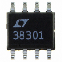
LTC3830-1ES8 Linear Technology, LTC3830-1ES8 Datasheet - Page 17

LTC3830-1ES8
Manufacturer Part Number
LTC3830-1ES8
Description
IC DC/DC CONTRLR STEP-DWN 8-SOIC
Manufacturer
Linear Technology
Type
Step-Down (Buck)r
Datasheet
1.LTC3830ES8.pdf
(24 pages)
Specifications of LTC3830-1ES8
Internal Switch(s)
No
Synchronous Rectifier
Yes
Number Of Outputs
1
Voltage - Output
3.3V, Adj
Current - Output
20A
Frequency - Switching
200kHz
Voltage - Input
3 ~ 8 V
Operating Temperature
-40°C ~ 85°C
Mounting Type
Surface Mount
Package / Case
8-SOIC (3.9mm Width)
Lead Free Status / RoHS Status
Contains lead / RoHS non-compliant
Power - Output
-
Other names
LTC38301ES8
Available stocks
Company
Part Number
Manufacturer
Quantity
Price
Company:
Part Number:
LTC3830-1ES8
Manufacturer:
LT
Quantity:
10 000
Company:
Part Number:
LTC3830-1ES8#PBF
Manufacturer:
TI
Quantity:
1 200
Company:
Part Number:
LTC3830-1ES8#TRPBF
Manufacturer:
LT
Quantity:
4 420
APPLICATIO S I FOR ATIO
Figure 10b shows the Bode plot of the overall transfer
function.
When low ESR output capacitors (Sanyo OS-CON) are
used, the ESR zero can be high enough in frequency that
it provides little phase boost at the loop crossover fre-
quency. As a result, the phase margin becomes inad-
equate and the load transient is not optimized. To resolve
this problem, a small capacitor can be connected between
the top of the resistor divider network and the V
create a pole-zero pair in the loop compensation. The zero
location is prior to the pole location and thus, phase lead
can be added to boost the phase margin at the loop
crossover frequency. The pole and zero locations are
located at:
where R1||R2 is the parallel combination resistance of R1
and R2. Choose C2 so that the zero is located at a lower
frequency compared to f
enough that the closed loop has enough phase margin for
stability. Figure 10c shows the Bode plot using phase
lead compensation around the LTC3830 resistor divider
network. Note: This technique is effective only when
R1 >> R2 i.e., at high output voltages only so that the pole
and zero are sufficiently separated.
Figure 10b. Bode Plot of the LTC3830 Overall Transfer Function
f
f
ZC2
PC2
= 1/[2π(R2)(C2)] and
= 1/[2π(R1||R2)(C2)]
f
Z
f
LC
U
f
ESR
CO
U
f
f
and the pole location is high
SW
CO
= CLOSED-LOOP CROSSOVER
= LTC3830 SWITCHING
f
FREQUENCY
FREQUENCY
CO
20dB/DECADE
W
f
P
FREQUENCY
3830 F10b
U
FB
pin to
Although a mathematical approach to frequency compen-
sation can be used, the added complication of input and/or
output filters, unknown capacitor ESR, and gross operat-
ing point changes with input voltage, load current varia-
tions, all suggest a more practical empirical method. This
can be done by injecting a transient current at the load and
using an RC network box to iterate toward the final values,
or by obtaining the optimum loop response using a
network analyzer to find the actual loop poles and zeros.
Table 2 shows the suggested compensation component
value for 5V to 3.3V applications based on Sanyo OS-CON
4SP820M low ESR output capacitors.
Table 2. Recommended Compensation Network for 5V to 3.3V
Applications Using Multiple Paralleled 820µF Sanyo OS-CON
4SP820M Output Capacitors
L1 (µH)
1.2
1.2
1.2
2.4
2.4
2.4
4.7
4.7
4.7
Figure 10c. Bode Plot of the LTC3830 Overall
Transfer Function Using a Low ESR Output Capacitor
C
f
Z
OUT
1640
2460
4100
1640
2460
4100
1640
2460
4100
f
LC
(µF)
LTC3830/LTC3830-1
f
R
ZC2
C
6.2
12
12
15
20
36
30
36
82
(kΩ)
f
f
SW
CO
= CLOSED-LOOP CROSSOVER
= LTC3830 SWITCHING
FREQUENCY
FREQUENCY
20dB/DECADE
C
C
f
f
3.3
3.3
1.8
2.7
1.0
1.0
1.8
1.0
1.0
ESR
CO
(nF)
f
P
C1 (pF)
f
PC2
470
470
220
330
220
220
330
180
180
3830 F10c
FREQUENCY
C2 (pF)
17
1000
1000
1000
1000
1000
1000
1000
1000
1000
3830fa


