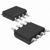
MAX766ESA+ Maxim Integrated Products, MAX766ESA+ Datasheet - Page 2

MAX766ESA+
Manufacturer Part Number
MAX766ESA+
Description
IC DC-DC INV HI EFF 8-SOIC
Manufacturer
Maxim Integrated Products
Type
Invertingr
Datasheet
1.MAX766CPA.pdf
(12 pages)
Specifications of MAX766ESA+
Internal Switch(s)
Yes
Synchronous Rectifier
No
Number Of Outputs
1
Voltage - Output
-15V, -1 ~ -16 V
Current - Output
105mA
Frequency - Switching
300kHz
Voltage - Input
3 ~ 16 V
Operating Temperature
-40°C ~ 85°C
Mounting Type
Surface Mount
Package / Case
8-SOIC (3.9mm Width)
Power - Output
471mW
Output Voltage
- 15 V
Output Current
0.1 A
Input Voltage
3 V to 16.5 V
Switching Frequency
300 KHz
Maximum Operating Temperature
+ 85 C
Mounting Style
SMD/SMT
Minimum Operating Temperature
- 40 C
Lead Free Status / RoHS Status
Lead free / RoHS Compliant
ABSOLUTE MAXIMUM RATINGS
V+ to GND ..............................................................-0.3V to +17V
OUT to GND ...........................................................+0.5V to -17V
Maximum Differential (V+ to OUT) ......................................+21V
REF, SHDN, FB to GND ...............................-0.3V to (V+ + 0.3V)
LX to V+..................................................................+0.3V to -21V
LX Peak Current ...................................................................1.5A
Continuous Power Dissipation (T
ELECTRICAL CHARACTERISTICS
(V+ = 5V, I
-5V/-12V/-15V or Adjustable,
High-Efficiency, Low I
Stresses beyond those listed under “Absolute Maximum Ratings” may cause permanent damage to the device. These are stress ratings only, and functional
operation of the device at these or any other conditions beyond those indicated in the operational sections of the specifications is not implied. Exposure to
absolute maximum rating conditions for extended periods may affect device reliability.
2
V+ Input Voltage Range
Supply Current
Shutdown Current
FB Trip Point
FB Input Current
Output Current and Voltage
(Note 1)
Reference Voltage
REF Load Regulation
REF Line Regulation
Load Regulation (Note 2)
Line Regulation (Note 2)
Efficiency (Note 2)
SHDN Leakage Current
SHDN Input Voltage High
SHDN Input Voltage Low
Plastic DIP (derate 9.09mW/°C above +70°C) ............727mW
SO (derate 5.88mW/°C above +70°C) .........................471mW
CERDIP (derate 8.00mW/°C above +70°C) .................640mW
_______________________________________________________________________________________
PARAMETER
LOAD
= 0mA, C
REF
= 0.1µF, T
A
= +70°C)
SYMBOL
I
SHDN
I
V
OUT
V
V+
I
V
REF
I
FB
S
IH
IL
A
= T
MIN
MAX76_C/E
MAX76_M
V+ = 16V, SHDN < 0.4V
V+ = 16V, SHDN > 1.6V
V+ = 10V, SHDN > 1.6V
3V ≤ V+ ≤ 16V
MAX76_C
MAX76_E
MAX76_M
MAX764, -4.8V ≤ V
MAX765C/E, -11.52V ≤ V
MAX765M, -11.52V ≤ V
MAX766, -14.40V ≤ V
MAX76_C
MAX76_E
MAX76_M
0µA ≤ I
3V ≤ V+ ≤ 16V
0mA ≤ I
4V ≤ V+ ≤ 6V
10mA ≤ I
V
V+ = 16V, SHDN = 0V or V+
3V ≤ V+ ≤ 16V
3V ≤ V+ ≤ 16V
IN
to T
= 5V
MAX
REF
LOAD
LOAD
, unless otherwise noted. Typical values are at T
≤ 100µA
≤ 100mA
Q
≤ 100mA,
CONDITIONS
OUT
DC-DC Inverters
OUT
Operating Temperature Ranges
Maximum Junction Temperatures
Storage Temperature Range ............................-65°C to +160°C
Lead Temperature (soldering, 10sec) ............................+300°C
OUT
≤ 5.2V
MAX76_C_A ........................................................0°C to +70°C
MAX76_E_A .....................................................-40°C to +85°C
MAX76_MJA ..................................................-55°C to +125°C
MAX76_C_A/E_A ..........................................................+150°C
MAX76_MJA .................................................................+175°C
OUT
MAX76_C/E
MAX76_M
V
V
≤ -15.60V
OUT
OUT
≤ 12.48V
≤ 12.48V
= -5V
= -15V
1.4700
1.4625
1.4550
MIN
150
3.0
3.5
-10
1.6
68
50
35
A
= +25°C.)
0.008
TYP
0.12
260
120
120
105
1.5
1.5
1.5
90
40
80
82
2
1
4
4
1.5300
1.5375
1.5450
MAX
16.0
±50
±70
±90
120
100
0.4
±1
10
10
15
5
UNITS
%/mA
µV/V
%/V
mA
mV
mV
µA
nA
µA
%
V
V
V
V


