LM2574N-3.3G ON Semiconductor, LM2574N-3.3G Datasheet
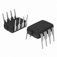
IC REG SW 0.5A 3.3V OUTPUT 8-DIP

LM2574N-3.3G

Manufacturer Part Number
LM2574N-3.3G
Description
IC REG SW 0.5A 3.3V OUTPUT 8-DIP
Manufacturer
ON Semiconductor
Type
Step-Down (Buck)r
Datasheets

Specifications of LM2574N-3.3G

Internal Switch(s)
Yes
Synchronous Rectifier
No
Number Of Outputs
1
Voltage - Output
3.3V
Current - Output
500mA
Frequency - Switching
52kHz
Voltage - Input
4.75 ~ 40 V
Operating Temperature
-40°C ~ 125°C
Mounting Type
Through Hole
Package / Case
8-DIP (0.300", 7.62mm)
Output Voltage
3.3 V
Output Current
0.5 A
Input Voltage
4.75 V to 40 V
Switching Frequency
52 KHz
Operating Temperature Range
- 40 C to + 125 C
Mounting Style
Through Hole
Duty Cycle (max)
98 %
Current, Input Bias
25 nA
Current, Output
0.5 A
Current, Supply
5 mA
Frequency, Oscillator
52 kHz
Package Type
PDIP-8
Regulator Type
Switching
Resistance, Thermal, Junction To Case
5 °C/W
Temperature, Operating, Range
-40 to +125 °C
Voltage, Output
3.3 V
Voltage, Supply
40 V
Lead Free Status / RoHS Status
Lead free / RoHS Compliant
Power - Output
-
Lead Free Status / Rohs Status
Lead free / RoHS Compliant
Other names
LM2574N-3.3G
LM2574N-3.3GOS
LM2574, NCV2574
0.5 A, Adjustable Output
Voltage, Step−Down
Switching Regulator
ideally suited for easy and convenient design of a step−down
switching regulator (buck converter). All circuits of this series are
capable of driving a 0.5 A load with excellent line and load regulation.
These devices are available in fixed output voltages of 3.3 V, 5.0 V,
12 V, 15 V, and an adjustable output version.
components to simplify the power supply design. Standard series of
inductors optimized for use with the LM2574 are offered by several
different inductor manufacturers.
efficiency is significantly higher in comparison with popular
three−terminal linear regulators, especially with higher input voltages.
In most cases, the power dissipated by the LM2574 regulator is so low,
that the copper traces on the printed circuit board are normally the only
heatsink needed and no additional heatsinking is required.
voltage within specified input voltages and output load conditions, and
±10% on the oscillator frequency (±2% over 0°C to +125°C). External
shutdown is included, featuring 60 mA (typical) standby current. The
output switch includes cycle−by−cycle current limiting, as well as
thermal shutdown for full protection under fault conditions.
Features
Applications
*For additional information on our Pb−Free strategy and soldering details, please download the ON Semiconductor Soldering and Mounting
© Semiconductor Components Industries, LLC, 2006
Techniques Reference Manual, SOLDERRM/D.
The LM2574 series of regulators are monolithic integrated circuits
These regulators were designed to minimize the number of external
Since the LM2574 converter is a switch−mode power supply, its
The LM2574 features include a guaranteed ±4% tolerance on output
over Line and Load Conditions
and Control Changes
3.3 V, 5.0 V, 12 V, 15 V, and Adjustable Output Versions
Adjustable Version Output Voltage Range, 1.23 to 37 V ±4% max
Guaranteed 0.5 A Output Current
Wide Input Voltage Range: 4.75 to 40 V
Requires Only 4 External Components
52 kHz Fixed Frequency Internal Oscillator
TTL Shutdown Capability, Low Power Standby Mode
High Efficiency
Uses Readily Available Standard Inductors
Thermal Shutdown and Current Limit Protection
NCV Prefix for Automotive and Other Applications Requiring Site
Pb−Free Packages are Available*
Simple and High−Efficiency Step−Down (Buck) Regulators
Efficient Pre−regulator for Linear Regulators
On−Card Switching Regulators
Positive to Negative Converters (Buck−Boost)
Negative Step−Up Converters
Power Supply for Battery Chargers
1
See detailed ordering and shipping information in the package
dimensions section on page 24 of this data sheet.
See general marking information in the device marking
section on page 24 of this data sheet.
* No internal connection, but should be soldered to
*
PC board for best heat transfer.
DEVICE MARKING INFORMATION
16
8
ORDERING INFORMATION
1
Pwr Gnd
Pwr Gnd
ON/OFF
ON/OFF
Sig Gnd
Sig Gnd
PIN CONNECTIONS
1
FB
FB
*
*
*
*
1
2
3
4
5
6
7
8
1
2
3
4
(Top View)
(Top View)
Publication Order Number:
16
15
14
13
12
11
10
9
8
7
6
5
DW SUFFIX
CASE 751G
CASE 626
N SUFFIX
SO−16 WB
PDIP−8
*
*
Output
*
V
*
*
*
*
Output
*
V
in
in
LM2574/D

Related parts for LM2574N-3.3G

LM2574N-3.3G Summary of contents

Page 1

... Positive to Negative Converters (Buck−Boost) • Negative Step−Up Converters • Power Supply for Battery Chargers *For additional information on our Pb−Free strategy and soldering details, please download the ON Semiconductor Soldering and Mounting Techniques Reference Manual, SOLDERRM/D. © Semiconductor Components Industries, LLC, 2006 16 1 ...

Page 2

Typical Application (Fixed Output Voltage Versions) 7.0 − Unregulated DC Input Representative Block Diagram and Typical Application +V in Unregulated DC Input 5 (12 (3) Feedback R2 Fixed Gain Error Amplifier ...

Page 3

OPERATING RATINGS (Operating Ratings indicate conditions for which the device is intended to be functional, but do not guarantee specific performance limits. For guaranteed specifications and test conditions, see the Electrical Characteristics). Rating Operating Junction Temperature Range Supply Voltage SYSTEM ...

Page 4

SYSTEM PARAMETERS ([Note 3] Test Circuit Figure 16) ELECTRICAL CHARACTERISTICS (continued) Adjustable version for the 12 V version min/max values T is the operating junction temperature range that applies [Note 4], unless otherwise noted). ...

Page 5

... NCV2574DW−ADJR2G LM2574N−3.3 3.3 V LM2574N−3.3G LM2574N−5 5.0 V LM2574N−5G LM2574N− LM2574N−12G LM2574N− LM2574N−15G †For information on tape and reel specifications, including part orientation and tape sizes, please refer to our Tape and Reel Packaging Specifications Brochure, BRD8011/D. ...

Page 6

16X 0. 14X −B− −A− NOTE 2 C −T− N SEATING PLANE 0.13 (0.005) M ...

Related keywords