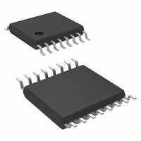
LM20136MH/NOPB National Semiconductor, LM20136MH/NOPB Datasheet - Page 4

LM20136MH/NOPB
Manufacturer Part Number
LM20136MH/NOPB
Description
IC REG SYNC BUCK 6A 16-TSSOP
Manufacturer
National Semiconductor
Series
PowerWise®r
Type
Step-Down (Buck)r
Datasheet
1.LM20136MHNOPB.pdf
(22 pages)
Specifications of LM20136MH/NOPB
Design Resources
LM20136 Design Spreadsheet
Internal Switch(s)
Yes
Synchronous Rectifier
Yes
Number Of Outputs
1
Voltage - Output
0.8 ~ 5 V
Current - Output
6A
Frequency - Switching
410kHz
Voltage - Input
2.95 ~ 5.5 V
Operating Temperature
-40°C ~ 125°C
Mounting Type
Surface Mount
Package / Case
16-TSSOP Exposed Pad, 16-eTSSOP, 16-HTSSOP
Power - Output
2.6W
Lead Free Status / RoHS Status
Lead free / RoHS Compliant
Other names
LM20136MH
www.national.com
Enable
Thermal Shutdown
Thermal Resistance
Note 1: Absolute Maximum Ratings indicate limits beyond which damage to the device may occur. Operating Ratings indicate conditions for which the device is
intended to be functional, but do not guarantee specific performance limits. For guaranteed specifications and test conditions, see the Electrical Characteristics.
Note 2: The maximum allowable power dissipation is a function of the maximum junction temperature, T
and the ambient temperature, T
maximum power dissipations of 2.6W is determined using T
characteristics table is measured with the part surface mounted to a 2" x 2" FR4 4 layer board. See Figure 10 for more detailed θ
Note 3: The human body model is a 100 pF capacitor discharged through a 1.5 kΩ resistor to each pin.
Typical Performance Characteristics
SPM6530T-1R0M120), V
waveforms, and T
Symbol
V
T
V
SD_HYS
EN_HYS
Efficiency vs. Load Current (V
T
IH_EN
θ
Efficiency vs. Load Current (V
SD
JA
Parameter
EN Pin Turn on Threshold
EN Pin Hysteresis
Thermal Shutdown
Thermal Shutdown Hysteresis
Junction to Ambient
J
= 25°C for all others.
IN
A
. The maximum allowable power dissipation at any ambient temperature is calculated using: P
= 5V, V
OUT
IN
IN
= 5V, f
= 1.2V, R
= 5V, f
SW
SW
A
LOAD
= 500 kHz)
= 25°C, θ
30053963
= 1 MHz)
30053965
= 1.2Ω, f
JA
= 25°C/W, and T
SW
Conditions
V
(Note 2)
4
Unless otherwise specified: C
EN
= 1 MHz, T
Efficiency vs. Load Current (V
Rising
Efficiency vs. Load Current (V
J_MAX
A
= 125°C. The θ
= 25°C for efficiency curves, loop gain plots and
J_MAX
, the junctions-to-ambient thermal resistance, θ
JA
specification of 25°C/W listed in the electrical
IN
= C
OUT
IN
IN
1.08
= 3.3V, f
Min
D_MAX
= 3.3V, f
= 100µF, L = 1.0µH (TDK
JA
information.
= (T
1.18
Typ
160
66
10
25
SW
J_MAX
SW
= 500 kHz)
30053966
30053964
= 1 MHz)
– T
Max
1.28
A
)/θ
JA
. The
°C/W
Unit
mV
°C
°C
V
JA
,


