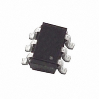
ZXSC420E6TA Diodes Zetex, ZXSC420E6TA Datasheet - Page 7

ZXSC420E6TA
Manufacturer Part Number
ZXSC420E6TA
Description
IC CONVERTER BOOST SOT23-6
Manufacturer
Diodes Zetex
Type
Step-Up (Boost)r
Datasheet
1.ZXSC410E6TA.pdf
(12 pages)
Specifications of ZXSC420E6TA
Internal Switch(s)
No
Synchronous Rectifier
No
Number Of Outputs
1
Voltage - Output
Adjustable
Current - Output
300mA
Frequency - Switching
Up to 200kHz
Voltage - Input
1.8 ~ 8 V
Operating Temperature
-40°C ~ 85°C
Mounting Type
Surface Mount
Package / Case
SOT-23-6
Power - Output
450mW
Lead Free Status / RoHS Status
Lead free / RoHS Compliant
Other names
ZXSC420E6TATR
Available stocks
Company
Part Number
Manufacturer
Quantity
Price
Part Number:
ZXSC420E6TA
Manufacturer:
ZETEX
Quantity:
20 000
Output voltage adjustment
The ZXSC410/420 are adjustable output converters
allowing the end user the maximum flexibilty. For
adjustable operation a potential divider network is
connected as follows:
The output voltage is determined by the equation:
V
where V
The resistor values, RA and RB, should be maximised
to improve efficiency and decrease battery drain.
Optimisation can be achieved by providing a minimum
current of I
adjustable from V
transistor, Q1.
Note: For the reference designs, RA is assigned the
label R2 and RB the label R3.
CONNECTION DIAGRAMS
ZXSC410
SOT23-6
ISSUE 2 - May 2003
OUT
V
V
FB
FB
FB
=300mV
STDN
FB(MAX)
1
GND
V
RA
RB
CC
FB
=200nA to the V
to the (BR)VCEO of the switching
V
GND
OUT
R
R
A
B
DRIVE
V
SENSE
FB
FB
pin. Output is
7
Layout issues
Layout is critical for the circuit to function in the most
efficient manner in terms of electrical efficiency,
thermal considerations and noise.
For ‘step-up converters’ there are four main current
loops, the input loop, power-switch loop, rectifier loop
and output loop. The supply charging the input
capacitor forms the input loop. The power-switch loop
is defined when Q1 is ‘on’, current flows from the input
through the inductor, Q1, R
Q1 is ‘off’, the energy stored in the inductor is
transferred to the output capacitor and load via D1,
forming the rectifier loop. The output loop is formed by
the output capacitor supplying the load when Q1 is
switched back off.
To optimise for best performance each of these loops
kept separate from each other and interconnected with
short, thick traces thus minimising parasitic
inductance, capacitance and resistance. Also the
R
trace length, between emitter lead of Q1 and ground,
again minimising stray parasitics.
ZXSC420
SOT23-6
SENSE
resistor should be connected, with minimum
GND
EOR
V
CC
SENSE
S E M I C O N D U C T O R S
DRIVE
V
SENSE
and to ground. When
FB
ZXSC410
ZXSC420


