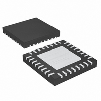
MAX1901ETJ+ Maxim Integrated Products, MAX1901ETJ+ Datasheet - Page 22

MAX1901ETJ+
Manufacturer Part Number
MAX1901ETJ+
Description
IC CNTRLR PWR SPLY LN 32-TQFN
Manufacturer
Maxim Integrated Products
Datasheet
1.MAX1904ETJ.pdf
(33 pages)
Specifications of MAX1901ETJ+
Applications
Controller, Notebook Computers
Voltage - Input
4.2 ~ 30 V
Number Of Outputs
4
Voltage - Output
2.5 ~ 5 V
Operating Temperature
0°C ~ 85°C
Mounting Type
Surface Mount
Package / Case
32-TQFN Exposed Pad
Output Voltage
3.3 V, 5 V, 2.5 V to 5.5 V
Output Current
5 A
Input Voltage
4.2 V to 30 V
Mounting Style
SMD/SMT
Maximum Operating Temperature
+ 85 C
Minimum Operating Temperature
- 40 C
Lead Free Status / RoHS Status
Lead free / RoHS Compliant
Therefore, when V
Bypass the V+ input with a 4.7µF tantalum capacitor
paralleled with a 0.1µF ceramic capacitor, close to the
IC. A 10Ω series resistor to V
Bypass the VL output with a 4.7µF tantalum capacitor
paralleled with a 0.1µF ceramic capacitor, close to the
device.
The output-filter capacitor values are generally deter-
mined by the ESR and voltage-rating requirements,
rather than actual capacitance requirements for loop sta-
bility. In other words, the low-ESR electrolytic capacitor
that meets the ESR requirement usually has more output
capacitance than is required for AC stability. Use only
specialized low-ESR capacitors intended for switching-
regulator applications, such as AVX TPS, Sanyo
POSCAP, or Kemet T510. To ensure stability, the capaci-
tor must meet both minimum capacitance and maximum
ESR values as given in the following equations:
These equations are worst case, with 45° of phase mar-
gin to ensure jitter-free, fixed-frequency operation and
provide a nicely damped output response for zero to
full-load step changes. Some cost-conscious designers
may wish to bend these rules with less-expensive
capacitors, particularly if the load lacks large step
changes. This practice is tolerable if some bench test-
ing over temperature is done to verify acceptable noise
and transient response.
No well-defined boundary exists between stable and
unstable operation. As phase margin is reduced, the
first symptom is a bit of timing jitter, which shows up as
blurred edges in the switching waveforms where the
500kHz Multi-Output, Low-Noise Power-Supply
Controllers for Notebook Computers
22
______________________________________________________________________________________
I
C
RMS
OUT
=
I
LOAD
>
V
R
Output-Filter Capacitor Value
IN
REF
ESR
V
×
is 2 x V
I
OUT
RMS
(
1
<
V
+
OUT
R
V
×
=
SENSE
OUT
R
OUT
I
LOAD
(
IN
SENSE
V
V
IN
IN
2
V
is also recommended.
/
REF
:
-
V
V
IN MIN
×
OUT
V
(
×
OUT
f
)
Bypassing V+
Bypassing VL
)
)
scope won’t quite sync up. Technically speaking, this
jitter (usually harmless) is unstable operation, since the
duty factor varies slightly. As capacitors with higher
ESRs are used, the jitter becomes more pronounced, and
the load-transient output-voltage waveform starts looking
ragged at the edges. Eventually, the load-transient wave-
form has enough ringing on it that the peak noise levels
exceed the allowable output-voltage tolerance. Note that
even with zero phase margin and gross instability pre-
sent, the output-voltage noise never gets much worse
than I
The output-voltage ripple is usually dominated by the
filter capacitor’s ESR, and can be approximated as
I
full equation for ripple in continuous-conduction mode
is V
C
discontinuous, with high peaks and widely spaced
pulses, so the noise can actually be higher at light load
(compared to full load). In idle mode, calculate the out-
put ripple as follows:
Buck-plus-flyback applications, sometimes called “cou-
pled-inductor” topologies, need a transformer to gener-
ate multiple output voltages. Performing the basic
electrical design is a simple task of calculating turns
ratios and adding the power delivered to the secondary
to calculate the current-sense resistor and primary
inductance. However, extremes of low input-output dif-
ferentials, widely different output loading levels, and
high turns ratios can complicate the design due to par-
asitic transformer parameters such as interwinding
capacitance, secondary resistance, and leakage
inductance. For examples of what is possible with real
world transformers, see the Maximum V
Current vs. Input Voltage graph in the Typical
Operating Characteristics.
Power from the main and secondary outputs is combined
to get an equivalent current referred to the main output
voltage (see the Inductor Value section for parameter
definitions). Set the current-sense resistor value at 80mV
/ I
RIPPLE
OUT
TOTAL
NOISE (p-p)
PEAK
)]. In idle mode, the inductor current becomes
.
✕
V
R
0 0003
✕
NOISE P P
.
ESR
R
ESR
. There is also a capacitive term, so the
(
= I
× ×
(under constant loads).
-
L
R
)
RIPPLE
(for Auxiliary Outputs Only)
SENSE
=
[ /
1
0 025
.
V
R
OUT
SENSE
2
✕
×
×
Transformer Design
C
[R
+
R
OUT
1
ESR
ESR
/(
V
IN
+
+ 1/(2
-
V
OUT
DD
)]
✕
π
Output
✕
f
✕


