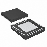
MAX1584ETJ+ Maxim Integrated Products, MAX1584ETJ+ Datasheet - Page 22

MAX1584ETJ+
Manufacturer Part Number
MAX1584ETJ+
Description
IC DGTL CAM PWR-SUP 5CH 32TQFN
Manufacturer
Maxim Integrated Products
Datasheet
1.MAX1585ETJ.pdf
(29 pages)
Specifications of MAX1584ETJ+
Applications
Controller, Digital Camera
Voltage - Input
0.7 ~ 5.5 V
Number Of Outputs
5
Voltage - Output
1.25 ~ 5.5 V
Operating Temperature
-40°C ~ 85°C
Mounting Type
Surface Mount
Package / Case
32-TQFN Exposed Pad
Lead Free Status / RoHS Status
Lead free / RoHS Compliant
Significant MOSFET selection parameters are as fol-
lows:
• On-resistance (R
• Maximum drain-to-source voltage (V
• Total gate charge (Q
• Reverse transfer capacitance (C
DL1 and DL3 swing between PVSU and GND. DL2
swings between INDL2 and GND. Use a MOSFET with
on-resistance specified at or below the DL_ drive volt-
age. The gate charge, Q
associated with charging the gate and helps to predict
MOSFET transition time between on and off states.
MOSFET power dissipation is a combination of on-
resistance and transition losses. The on-resistance loss
is as follows:
where D is the duty cycle, I
current, and R
transition loss is approximately:
where V
inductor current, f
t
mately Q
I
dissipation in the MOSFET is as follows:
For most AUX applications, a Schottky diode rectifies
the output voltage. Schottky low forward voltage and
fast recovery time provide the best performance in
most applications. Silicon signal diodes (such as
1N4148) are sometimes adequate in low-current
(<10mA), high-voltage (>10V) output circuits where the
output voltage is large compared to the diode forward
voltage.
The auxiliary controllers employ voltage-mode control
to regulate their output voltage. Optimum compensa-
tion depends on whether the design uses continuous or
discontinuous inductor current.
When the inductor current falls to zero on each switch-
ing cycle, it is described as discontinuous. The inductor
is not utilized as efficiently as with continuous current,
but in light-load applications, this often has little nega-
tive impact since the coil losses may already be low
compared to other losses. A benefit of discontinuous
5-Channel Slim DSC Power Supplies
22
T
G
is the transition time. The transition time is approxi-
is the gate-drive current (0.5A typ). The total power
______________________________________________________________________________________
AUX Step-Up, Discontinuous Inductor Current
OUT
G
P
/ I
TRANS
P
G
P
is the output voltage, I
MOSFET
DS(ON)
RDSON
, where Q
= (V
OSC
DS(ON)
is the MOSFET on-resistance. The
= P
= D x I
OUT
is the switching frequency, and
G
G
)
RDSON
G
)
x I
is the total gate charge, and
, includes all capacitance
L
L
L
2
x f
is the average inductor
x R
+ P
OSC
AUX Compensation
DS(ON)
RSS
TRANS
x t
L
)
DS(MAX)
is the average
T
) / 3
)
Diode
inductor current is more flexible loop compensation, and
no maximum duty-cycle restriction on boost ratio.
To ensure discontinuous operation, the inductor must
have a sufficiently low inductance to fully discharge on
each cycle. This occurs when:
A discontinuous current boost has a single pole at the
following:
Choose the integrator cap so the unity-gain crossover,
f
such as those powering motors, LEDs, or other loads
that do not require fast transient response, it is often
acceptable to overcompensate by setting f
20 or lower.
C
where:
and V
The C
Continuous inductor current can sometimes improve
boost efficiency by lowering the ratio between peak
inductor current and output current. It does this at the
expense of a larger inductance value that requires larg-
er size for a given current rating. With continuous
inductor-current boost operation, there is a right-half-
plane zero, Z
where (1 - D) = V
There is a complex pole pair at the following:
If the zero due to the output capacitor capacitance and
ESR is less than 1/10 the right-half-plane zero:
Then choose C
at Z
crossover:
Choose R
C
C
C
C
C
, occurs at f
C
R
C
), at f
F
L < [V
is then determined by the following:
C
C
COUT
P
= [2V
Z
RAMP
C
= (V
= R
= (2V
(K(V
COUT
R
0
IN
C
R
AUX Step-Up, Continuous Inductor Current
to cancel one of the pole pairs:
LOAD
. The ESR zero provides a phase boost at
C
IN
OUT
f
0
C
2
OUT
zero is then used to cancel the f
OUT
is the internal voltage ramp of 1.25V.
Z
to place the integrator zero, 1 / (2π x R
= V
/ V
(V
= V
RHP
= 1 / (2π x C
RHP
OSC
x V
OUT
RAMP
C
x C
- V
OUT
- V
IN
K = 2L x f
, at the following:
IN
= (1 - D)
so the crossover frequency f
IN
IN
/ 10 or lower. For many AUX circuits,
(L x C
IN
OUT
/ V
- V
/ ((2V
))]
/ [2π x V
)(V
) / (2π x R
OUT
IN
1/2
FB
x V
) / V
OUT
OUT
OUT
[(V
2
OSC
/ V
OUT
(in a boost converter)
R
OUT
FB
IN
)
LOAD
OUT
1/2
x R
- V
LOAD
/ R
/ [(2V
(L x C
/ V
3
/ (V
)(g
IN
] [R
ESR
LOAD
OUT
) x V
/ (2π x L)
M
OUT
x C
OUT
LOAD
) < Z
OUT
/ (2π x Z
)(g
RAMP
OUT
x C
M
- V
)
RHP
1/2
/ (2f
P
/ (2π x f
C
IN
C
x V
]
)] [V
pole, so:
)
) x C
/ 10
COUT
OSC
at f
C
OUT
occurs
OUT
OSC
)]
C
C
)
))
]
))]
C
/
x
/


