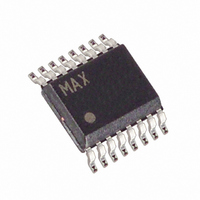
MAX1809ETI+T Maxim Integrated Products, MAX1809ETI+T Datasheet - Page 13

MAX1809ETI+T
Manufacturer Part Number
MAX1809ETI+T
Description
IC DDR TERMINATION 28-TQFN
Manufacturer
Maxim Integrated Products
Datasheet
1.MAX1809EEE.pdf
(17 pages)
Specifications of MAX1809ETI+T
Applications
Converter, DDR
Voltage - Input
3 ~ 5.5 V
Number Of Outputs
1
Voltage - Output
1.1 ~ 5.5 V
Operating Temperature
0°C ~ 85°C
Mounting Type
Surface Mount
Package / Case
16-QSOP
Lead Free Status / RoHS Status
Lead free / RoHS Compliant
the dissipation in the termination resistor is halved com-
pared to a termination scheme that connects the resistive
terminators to ground.
The V
memory voltage (V
memory voltage, and is able to source and sink current
depending on the state of the bus. These requirements
are met in the MAX1809.
When SHDN is brought low after the controller has
been on for a while, the output may remain high if there
is no leakage or discharge path to bring the output
down. For DDR memory systems, keeping V
when V
fications. This can result in the bus latching if the sys-
Figure 9. Discharging the Output of the MAX1809 in Shutdown
Figure 10. Starting the MAX1809 in Sinking Mode with V
>V
INPUT VOLTAGE
(3V TO 5.5V)
2.2µF
EXTREF
10Ω
TT
DDQ
Discharging the Output in Shutdown
supply requires that it regulates to half the
C
SHDN
IN
3A, 1MHz, DDR Memory Termination Supply
(2.5V) is shut down violates the DDR speci-
INPUT VOLTAGE
(3V TO 5.5V)
2.2µF
IN
V
SHDN
CC
10Ω
______________________________________________________________________________________
DDQ
MAX1809
C
SHDN
), tracks the changes of the
IN
PGND
GND
LX
FB
SS
IN
V
SHDN
CC
MAX1809
0.01µF
L
100Ω
EXTREF
PGND
GND
TT
LX
FB
C
OUT
V
at 1.25V
TT
OUT
=V
DDQ
V
(2.5V)
/2
DDQ
V
10kΩ
10kΩ
SSQ
L
C
OUT
tem is subsequently turned on or possibly damaging
the memory subsystem.
When using the MAX1809 to generate the V
1.25V, several circuits are recommended to discharge
the output when the MAX1809 is shut down. These are
shown in Figure 9. Solution (a) is a diode added from
V
goes low. Alternatively, solution (b) uses a small signal
transistor to discharge V
down.
The MAX1809 will not startup until the feedback voltage
is made less than the external reference voltage when
power is applied or when the part is exiting shutdown.
In applications that cannot guarantee V
TT
V
0.1µF
0.1µF
TOP VIEW
TT
to V
= V
Pin Configurations (continued)
DDQ
DDQ
/2
(a)
EXTREF
so that V
SHDN
TOFF
SS
LX
FB
IN
IN
2N7002
1
2
3
4
5
6
7
8
(b)
TT
Startup in Sinking Mode
MAX1809
TT
QSOP
is discharged when VDDQ
when the MAX1809 is shut
SHDN
16
15
14
13
12
11
10
9
LX
PGND
LX
PGND
V
GND
REF
GND
CC
FB
TT
< V
output of
EXTREF
13


