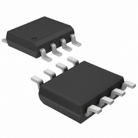
MAX607ESA Maxim Integrated Products, MAX607ESA Datasheet - Page 7

MAX607ESA
Manufacturer Part Number
MAX607ESA
Description
IC CONV DCDC F/FLASH MEM 8-SOIC
Manufacturer
Maxim Integrated Products
Datasheet
1.MAX606ESA.pdf
(12 pages)
Specifications of MAX607ESA
Applications
Converter, Flash Memory PCMCIA Cards
Voltage - Input
3 ~ 5.5 V
Number Of Outputs
1
Voltage - Output
12V, 3 ~ 12.5 V
Operating Temperature
0°C ~ 85°C
Mounting Type
Surface Mount
Package / Case
8-SOIC (3.9mm Width)
Lead Free Status / RoHS Status
Contains lead / RoHS non-compliant
Available stocks
Company
Part Number
Manufacturer
Quantity
Price
Part Number:
MAX607ESA
Manufacturer:
MAXIM/美信
Quantity:
20 000
Part Number:
MAX607ESA+
Manufacturer:
MAXIM/美信
Quantity:
20 000
Company:
Part Number:
MAX607ESA+T
Manufacturer:
Maxim
Quantity:
2 500
This data sheet provides two predesigned standard
application circuits. The circuit of Figure 1 produces 12V
at 120mA from a 5V input. Table 1 lists component val-
ues and part numbers for both the MAX606 and MAX607
variations of this circuit. The circuit of Figure 2 produces
Figure 1. 12V Standard Application Circuit
DC-DC Converters for Flash Memory/PCMCIA Cards
PIN
INPUT
C1
1
2
3
4
5
6
7
8
+5V
ON/OFF
Standard Application Circuits
C4
C2
NAME
PGND
SHDN
GND
OUT
FB
SS
LX
IN
SHDN
SS
FB
GND
_______________________________________________________________________________________
MAX606
MAX607
Power Ground. Source of n-channel power MOSFET.
Feedback Input. Connect to IN for 5V output, to GND for 12V output, or to a resistive voltage divider between
OUT and GND for an adjustable output between IN and 12.5V.
Shutdown Input, Active Low. Connect to GND to power down or to IN for normal operation. Output power FET
is held off when SHDN is low.
Supply Voltage Input: 3.0V to 5.5V
Analog Ground
Soft-Start Input
Output. Always connect directly to the circuit output.
Drain of n-channel power MOSFET
Low-Profile, 5V/12V or Adjustable, Step-Up
PGND
IN
OUT
LX
L1
D1
C3
12V @ 120mA
OUTPUT
5V at a typical output current of 180mA from a 3.3V
input. Each application circuit is designed to deliver the
full rated output load current over the temperature range
listed. Component values and part numbers for this cir-
cuit are listed in Table 2. See Table 3 for component
suppliers’ phone and fax numbers.
Figure 2. 5V Standard Application Circuit
FUNCTION
INPUT
+3.3V
C1
ON/OFF
C4
C2
SHDN
SS
GND
FB
MAX606
MAX607
PGND
IN
OUT
LX
Pin Description
L1
D1
C3
5V @ 180mA
OUTPUT
7


