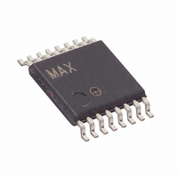
MAX1779EUE+T Maxim Integrated Products, MAX1779EUE+T Datasheet

MAX1779EUE+T
Specifications of MAX1779EUE+T
Related parts for MAX1779EUE+T
MAX1779EUE+T Summary of contents
Page 1
... PDAs Digital-Still Cameras Camcorders Typical Operating Circuit appears at end of data sheet. ________________________________________________________________ Maxim Integrated Products For pricing, delivery, and ordering information, please contact Maxim/Dallas Direct! at 1-888-629-4642, or visit Maxim’s website at www.maxim-ic.com. ♦ Three Integrated DC-DC Converters ♦ 250kHz Current-Mode PWM Boost Regulator Up to +13V Main High-Power Output ± ...
Page 2
Low-Power Triple-Output TFT LCD DC-DC Converter ABSOLUTE MAXIMUM RATINGS IN, SHDN, TGND to GND .........................................-0.3V to +6V DRVN to GND .........................................-0. DRVP to GND..........................................-0. PGND to GND.....................................................................±0.3V RDY to GND ...........................................................-0.3V to +14V LX, SUPP, SUPN ...
Page 3
Low-Power Triple-Output TFT LCD DC-DC ELECTRICAL CHARACTERISTICS (continued) = +3.0V, SHDN = IN SUPP SUPN unless otherwise noted. Typical values are at T PARAMETER SYMBOL Operating Frequency FBP Regulation Voltage V FBP Input Bias Current ...
Page 4
Low-Power Triple-Output TFT LCD DC-DC Converter ELECTRICAL CHARACTERISTICS = +3.0V, SHDN = IN SUPP SUPN unless otherwise noted.) (Note 1) PARAMETER SYMBOL Input Supply Range V Input Undervoltage Threshold V UVLO IN Quiescent Supply Current ...
Page 5
Low-Power Triple-Output TFT LCD DC-DC ELECTRICAL CHARACTERISTICS (continued) = +3.0V, SHDN = IN SUPP SUPN unless otherwise noted.) (Note 1) PARAMETER SYMBOL LOGIC SIGNALS SHDN Input Low Voltage SHDN Input High Voltage SHDN Input Current ...
Page 6
Low-Power Triple-Output TFT LCD DC-DC Converter (Circuit of Figure +3.3V +25°C, unless otherwise noted EFFICIENCY vs. LOAD CURRENT (BOOST CONVERTER AND CHARGE PUMPS) 100 V = +5V MAIN TWO-STAGE 90 CHARGE PUMPS 80 ...
Page 7
Low-Power Triple-Output TFT LCD DC-DC (Circuit of Figure +3.3V +25°C, unless otherwise noted LOAD TRANSIENT WITHOUT INTEGRATOR (L = 10μH, 500μs PULSE) MAX1779-16 5.0V 4.9V 50mA 0 100μs/div 5V, 50mV/div ...
Page 8
Low-Power Triple-Output TFT LCD DC-DC Converter (Circuit of Figure +3.3V +25°C, unless otherwise noted STARTUP WAVEFORM (L = 33μ 500mA 0 200μs/div 2V, 2V/div ...
Page 9
Low-Power Triple-Output TFT LCD DC-DC PIN NAME 10 DRVN Negative Charge-Pump Driver Output. Output high level SUPN Negative Charge-Pump Driver Supply Voltage. Bypass to PGND with a 0.1μF capacitor. 12 DRVP Positive Charge-Pump Driver Output. Output high ...
Page 10
Low-Power Triple-Output TFT LCD DC-DC Converter OSC - + - - + INTG C INTG Figure 1. PWM Boost Converter Block Diagram ( charge flows from until the C3 SUPP diode (D3) turns off. ...
Page 11
Low-Power Triple-Output TFT LCD DC-DC OSC MAX1779 Figure 2. Negative Charge-Pump Block Diagram OSC MAX1779 Figure 3. Positive Charge-Pump Block Diagram ______________________________________________________________________________________ SUPN C5 DRVN FBN + - - V REF + 1.25V REF GND PGND SUPP C3 DRVP FBP ...
Page 12
Low-Power Triple-Output TFT LCD DC-DC Converter 1.125V), the active-low ready signal (RDY) is pulled low (see Power Ready section). Power ready is an open-drain output. When the power- up sequence is properly completed, the MOSFET turns on and pulls RDY ...
Page 13
Low-Power Triple-Output TFT LCD DC-DC where R is the inductor’s series resistance. For best L performance, select inductors with resistance less than the internal N-channel MOSFET on-resistance (1Ω typ). The output capacitor selection depends on circuit sta- bility and output ...
Page 14
Low-Power Triple-Output TFT LCD DC-DC Converter nated by the internal switch resistance and the diode impedance. Start with 0.1µF ceramic capacitors. Smaller values may be used for low-current applica- tions. Charge-Pump Output Capacitor Increasing the output capacitance or decreasing the ...
Page 15
Low-Power Triple-Output TFT LCD DC-DC Figure 4. Minimizing the Number of Charge-Pump Stages ______________________________________________________________________________________ Converter 15 ...
Page 16
Low-Power Triple-Output TFT LCD DC-DC Converter Figure 5. Typical Operating Circuit (L = 33µH) 16 ______________________________________________________________________________________ ...
Page 17
Low-Power Triple-Output TFT LCD DC-DC Figure 6. Typical Operating Circuit (L = 10µH) ______________________________________________________________________________________ Converter 17 ...
Page 18
... Maxim cannot assume responsibility for use of any circuitry other than circuitry entirely embodied in a Maxim product. No circuit patent licenses are implied. Maxim reserves the right to change the circuitry and specifications without notice at any time. 18 ____________________Maxim Integrated Products, 120 San Gabriel Drive, Sunnyvale, CA 94086 408-737-7600 © 2005 Maxim Integrated Products Printed USA is a registered trademark of Maxim Integrated Products, Inc ...


