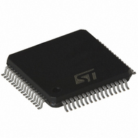
L6714 STMicroelectronics, L6714 Datasheet - Page 64

L6714
Manufacturer Part Number
L6714
Description
IC CTRLR 4PH W/DRIVERS 64-TQFP
Manufacturer
STMicroelectronics
Datasheet
1.L6714TR.pdf
(70 pages)
Specifications of L6714
Applications
Controller, Intel VR10, VR11, AMD CPU
Voltage - Input
12V
Number Of Outputs
4
Voltage - Output
0.3 ~ 1.6 V
Operating Temperature
0°C ~ 70°C
Mounting Type
Surface Mount
Package / Case
64-TQFP Exposed Pad, 64-eTQFP, 64-HTQFP, 64-VQFP
Mounting Style
SMD/SMT
Case
QFP
Lead Free Status / RoHS Status
Lead free / RoHS Compliant
Available stocks
Company
Part Number
Manufacturer
Quantity
Price
Company:
Part Number:
L6714TR
Manufacturer:
WYC
Quantity:
22 140
Part Number:
L6714TR
Manufacturer:
ST
Quantity:
20 000
Layout guidelines
24
24.1
64/70
Layout guidelines
Since the device manages control functions and high-current drivers, layout is one of the
most important things to consider when designing such high current applications. A good
layout solution can generate a benefit in lowering power dissipation on the power paths,
reducing radiation and a proper connection between signal and power ground can optimize
the performance of the control loops.
Two kind of critical components and connections have to be considered when layouting a
VRM based on L6714: power components and connections and small signal components
connections.
Power components and connections
These are the components and connections where switching and high continuous current
flows from the input to the load. The first priority when placing components has to be
reserved to this power section, minimizing the length of each connection and loop as much
as possible. To minimize noise and voltage spikes (EMI and losses) these interconnections
must be a part of a power plane and anyway realized by wide and thick copper traces: loop
must be anyway minimized. The critical components, i.e. the power transistors, must be
close one to the other. The use of multi-layer printed circuit board is recommended.
Figure 26
input capacitance (C
placed close to the power section in order to eliminate the stray inductance generated by the
copper traces. Low ESR and ESL capacitors are preferred, MLCC are suggested to be
connected near the HS drain.
Use proper VIAs number when power traces have to move between different planes on the
PCB in order to reduce both parasitic resistance and inductance. Moreover, reproducing the
same high-current trace on more than one PCB layer will reduce the parasitic resistance
associated to that connection.
Connect output bulk capacitor as near as possible to the load, minimizing parasitic
inductance and resistance associated to the copper trace also adding extra decoupling
capacitors along the way to the load when this results in being far from the bulk capacitor
bank.
Gate traces must be sized according to the driver RMS current delivered to the power
MOSFET. The device robustness allows managing applications with the power section far
from the controller without losing performances. External gate resistors help the device to
dissipate power resulting in a general cooling of the device. When driving multiple
MOSFETs in parallel, it is suggested to use one resistor for each MOSFET.
shows the details of the power connections involved and the current loops. The
IN
), or at least a portion of the total capacitance needed, has to be
L6714


