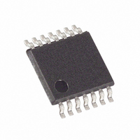
MAX3355EEUD+ Maxim Integrated Products, MAX3355EEUD+ Datasheet - Page 2

MAX3355EEUD+
Manufacturer Part Number
MAX3355EEUD+
Description
IC CHARGE PUMP USB OTG 14TSSOP
Manufacturer
Maxim Integrated Products
Datasheet
1.MAX3355EEUD.pdf
(11 pages)
Specifications of MAX3355EEUD+
Applications
Charge Pump, USB
Voltage - Input
2.6 ~ 5.5 V
Number Of Outputs
1
Operating Temperature
-40°C ~ 85°C
Mounting Type
Surface Mount
Package / Case
14-TSSOP
Maximum Operating Temperature
+ 85 C
Minimum Operating Temperature
- 40 C
Mounting Style
SMD/SMT
Lead Free Status / RoHS Status
Lead free / RoHS Compliant
Voltage - Output
-
Lead Free Status / Rohs Status
Lead free / RoHS Compliant
ABSOLUTE MAXIMUM RATINGS
(All voltages referenced to GND)
V
C+..................................................................(V
C-................................................................-0.3V to (V
OFFVBUS, SHDN, STATUS1,
V
Output Current (all other pins)..........................................±15mA
Continuous Power Dissipation (T
±15kV ESD-Protected USB On-the-Go
Charge Pump and Comparators in UCSP
Stresses beyond those listed under “Absolute Maximum Ratings” may cause permanent damage to the device. These are stress ratings only, and functional
operation of the device at these or any other conditions beyond those indicated in the operational sections of the specifications is not implied. Exposure to
absolute maximum rating conditions for extended periods may affect device reliability.
ELECTRICAL CHARACTERISTICS
(V
capacitor to GND, C
+25°C, unless otherwise noted.) (Notes 1, 2)
2
Supply Voltage
Logic Supply Voltage
Logic Supply Current
Operating Supply Current
Shutdown Supply Current
Thermal-Shutdown Protection
Threshold
Thermal-Shutdown Protection
Hysteresis
LOGIC INPUTS AND OUTPUTS
STATUS1, STATUS2, ID_OUT
Output Voltage
OFFVBUS, SHDN Input Voltage
Input Leakage Current
V
V
V
V
CC
BUS
CC
BUS
BUS
BUS
STATUS2, ID_OUT ....................................-0.3V to (V
4 x 3 UCSP (derate 6.5mW/°C above +70°C) .............520mW
BUS
, V
_______________________________________________________________________________________
Short Circuit to GND .........................................Continuous
= +2.6V to +5.5V, V
L
Output Voltage
Leakage Voltage
Sink Current
OUTPUT VOLTAGE: DEVICE A CONFIGURED
, V
BUS
PARAMETER
, ID_IN.............................................-0.3V to +6.0V
LOAD
= 1µF (min), ESR
L
= +1.65V to V
A
= +70°C)
SYMBOL
I
CCSHDN
V
I
V
V
LOAD
CC
I
V
LKG
V
V
CC
I
CC
OH
OL
IH
L
IL
L
CC
, C1 = 0.1µF, V
= 1Ω (max), T
- 0.3V) to +6V
CC
L
No activity on V
reference active
Device A configured, OFFVBUS = V
I
Device B configured, SHDN = GND
Device A configured, SHDN = GND
Device A configured, OFFVBUS = V
charge pump on
Device A configured, OFFVBUS = V
charge pump on
I
I
OFFVBUS, SHDN = GND or V
I
OFFVBUS = V
No load, C
ID_IN = GND
OFFVBUS = GND
OFFVBUS = GND, V
LOAD
SOURCE
SINK
LOAD
+ 0.3V)
+ 0.3V)
= -1mA
= 8mA, charge pump on
= 0 to 8mA, C
CC
A
= +1mA
LOAD
= T
decoupled with 1µF capacitor to GND, V
CONDITIONS
L
MIN
Operating Temperature Range ...........................-40°C to +85°C
Storage Temperature Range .............................-65°C to +150°C
Junction Temperature ......................................................+150°C
Lead Temperature (soldering, 10s) .................................+300°C
Bump Temperature (soldering)
, ID_IN = GND
BUS
= 1µF, OFFVBUS = V
14-Pin TSSOP (derate 9.1mW/°C above +70°C) .........727mW
Infrared (15s) ...............................................................+200°C
Vapor Phase (20s) .......................................................+215°C
to T
; comparator and
LOAD
BUS
MAX
= +6.0V
= 1µF,
. Typical values are at V
L
L
L
L
,
,
,
L
,
2/3 x V
2/3 x V
MIN
1.65
4.63
2.6
L
L
CC
+150
= +3.0V, V
TYP
+20
L
4.8
30
decoupled with 0.1µF
MAX
V
5.25
100
200
200
150
5.5
0.4
0.4
±1
20
L
CC
1
= 1.8V, T
UNITS
mA
mV
µA
µA
µA
°C
°C
µA
µA
V
V
V
V
V
A
=


