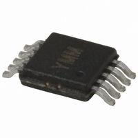
MIC2169BMM TR Micrel Inc, MIC2169BMM TR Datasheet - Page 13

MIC2169BMM TR
Manufacturer Part Number
MIC2169BMM TR
Description
IC CTRLR PWM SYNC BUCK 10-MSOP
Manufacturer
Micrel Inc
Datasheet
1.MIC2169YMM.pdf
(15 pages)
Specifications of MIC2169BMM TR
Pwm Type
Voltage Mode
Number Of Outputs
1
Frequency - Max
550kHz
Duty Cycle
92%
Voltage - Supply
3 V ~ 14.5 V
Buck
Yes
Boost
No
Flyback
No
Inverting
No
Doubler
No
Divider
No
Cuk
No
Isolated
No
Operating Temperature
-40°C ~ 85°C
Package / Case
10-MSOP, Micro10™, 10-uMAX, 10-uSOP
Frequency-max
550kHz
Lead Free Status / RoHS Status
Contains lead / RoHS non-compliant
Other names
MIC2169BMMTR
MIC2169BMMTR
MIC2169BMMTR
Design Example
Layout and Checklist:
March 2009
1. Connect the current limiting (R2) resistor directly
2. Use a 5Ω resistor from the input supply to the VIN
3. The feedback resistors R3 and R4/R5/R6 should
4. The compensation resistor and capacitors should
5. Add a 1.4Ω resistor and a 1000pF capacitor from
6. Add place holders for gate resistors on the top and
to the drain of top MOSFET Q3.
pin on the MIC2169. Also, place a 1μF ceramic
capacitor from this pin to GND, preferably not thru
a via.
be placed close to the FB pin. The top side of R3
should connect directly to the output node. Run
this trace away from the switch node (junction of
Q3, Q2, and L1). The bottom side of R3 should
connect to the GND pin on the MIC2169.
be placed right next to the COMP pin and the other
side should connect directly to the GND pin on the
MIC2169 rather than going to the plane.
the switch node to ground pin. See page 7, Current
Limiting section for more detail.
bottom MOSFET gate drives. If necessary, gate
resistors of 10Ω or less should be used.
SHDN
J1
+Vin 5-12V
J2
J3
GND
1
1
1
R7
100K
C14
DIN
R1
0 Ohm
68uF/20V
2N7002E
C2
1
Q1
Cin=AVX TPSD686M020R0070
+
20V
68uF
C3
C9
Open
1uF/16V
+
10uF/16V
C13
4.02K
C10
0.1uF
R8
C1
4
COMP/EN
R9
10
470 ohm
MIC2169BMM Evaluation Board Schematic
MIC2169
R2
C16
0.1uF
U1
VSW
HSD
BST
LSD
FB
C4
10uF/6V
10
9
8
7
5
R11
RES
R13
RES
SD103BWS
C5
0.1uF/25V
D1
13
4
R10
4R02 Ohm
4
IRF7821
7. Low gate charge MOSFETs should be used to
8. Compensation component GND, feedback resistor
9. The 10μF ceramic capacitor should be placed
10. The 10μF ceramic capacitor should be placed right
11. The source of the bottom MOSFET should connect
12. Place a 0.01μF to 0.1μF ceramic capacitor in parallel
Q2
+VIN
IRF7821
Q3
maximize effi ciency, such as Si4800, Si4804BDY,
IRF7821, IRF8910, FDS6680A and FDS6912A,
etc.
ground, chip ground should all run together and
connect to the output capacitor ground. See demo
board layout, top layer.
between the drain of the top MOSFET and the
source of the bottom MOSFET.
on the VDD pin without any vias.
directly to the input capacitor GND with a thick
trace. The output capacitor and the input capacitor
should connect directly to the GND plane.
with the CS resistor to fi lter any switching noise.
R12
47
C15
100pF
2
D2
L1
CDRH127 / LD-1R0-MC
1.0uH
330uF/6.3V
3.16k
C
3.3V
C6
R4
1
+
B
2.5V
330uF
Cout=AVX TPSD337M006R0045
C7
R5
4.64K
+
A
1.5V
Open
R6
11.3K
C8
JP2
HEADER 3X2
+
R3
10K
C11
Open
R14
Open
M9999-032409
0.1uF/25V
C12
J4
Vout
J5
GND
1
1


