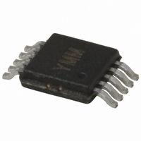
MIC2169BMM Micrel Inc, MIC2169BMM Datasheet - Page 10

MIC2169BMM
Manufacturer Part Number
MIC2169BMM
Description
IC CTRLR PWM SYNC BUCK 10-MSOP
Manufacturer
Micrel Inc
Datasheet
1.MIC2169YMM.pdf
(15 pages)
Specifications of MIC2169BMM
Pwm Type
Voltage Mode
Number Of Outputs
1
Frequency - Max
550kHz
Duty Cycle
92%
Voltage - Supply
3 V ~ 14.5 V
Buck
Yes
Boost
No
Flyback
No
Inverting
No
Doubler
No
Divider
No
Cuk
No
Isolated
No
Operating Temperature
-40°C ~ 85°C
Package / Case
10-MSOP, Micro10™, 10-uMAX, 10-uSOP
Frequency-max
550kHz
Lead Free Status / RoHS Status
Contains lead / RoHS non-compliant
Available stocks
Company
Part Number
Manufacturer
Quantity
Price
Company:
Part Number:
MIC2169BMM
Manufacturer:
MOSTEK
Quantity:
6 235
Part Number:
MIC2169BMM
Manufacturer:
MICREL/麦瑞
Quantity:
20 000
Part Number:
MIC2169BMMTR
Manufacturer:
MICROCHIP/微芯
Quantity:
20 000
Where:
The output voltage is determined by the equation:
A typical value of R1 can be between 3kΩ and 10kΩ. If R1 is
too large, it may allow noise to be introduced into the voltage
feedback loop. If R1 is too small, in value, it will decrease the
effi ciency of the power supply, especially at light loads. Once
R1 is selected, R2 can be calculated using:
External Schottky Diode
An external freewheeling diode is used to keep the inductor
current fl ow continuous while both MOSFETs are turned off.
This dead time prevents current from fl owing unimpeded
through both MOSFETs and is typically 15ns. The diode
conducts twice during each switching cycle. Although the
average current through this diode is small, the diode must
be able to handle the peak current.
The reverse voltage requirement of the diode is:
The power dissipated by the Schottky diode is:
where:
The external Schottky diode, D1, is not necessary for circuit
operation since the low-side MOSFET contains a parasitic
body diode. The external diode will improve effi ciency and
decrease high frequency noise. If the MOSFET body diode
is used, it must be rated to handle the peak and average cur-
rent. The body diode has a relatively slow reverse recovery
time and a relatively high forward voltage drop. The power
M9999-032409
V
V
REF
V
I
V
P
F
D(avg)
Figure 2. Voltage-Divider Confi guration
DIODE(rrm)
DIODE
O
= forward voltage at the peak diode current
R2
=
MIC2169 [adj.]
for the MIC2169 is typically 0.8V
V
REF
=
=
=
I
V
OUT
V
I
D(avg)
O
REF
×
Error
Amp
=
−
⎛
⎜
⎝
1
× ×
V
V
×
IN
+
REF
2 15ns f
×
R 1
R2
R1
V
0.8V
V
F
REF
⎞
⎟
⎠
×
S
FB
7
R1
R2
10
lost in the diode is proportional to the forward voltage drop
of the diode. As the high-side MOSFET starts to turn on, the
body diode becomes a short circuit for the reverse recovery
period, dissipating additional power. The diode recovery and
the circuit inductance will cause ringing during the high-side
MOSFET turn-on. An external Schottky diode conducts at
a lower forward voltage preventing the body diode in the
MOSFET from turning on. The lower forward voltage drop
dissipates less power than the body diode. The lack of a
reverse recovery mechanism in a Schottky diode causes
less ringing and less power loss. Depending upon the circuit
components and operating conditions, an external Schottky
diode will give a
Feedback Loop Compensation
The MIC2169 controller comes with an internal transcon-
ductance error amplifi er used for compensating the voltage
feedback loop by placing a capacitor (C1) in series with a
resistor (R1) and another capacitor C2 in parallel from the
COMP pin-to-ground. See “Functional Block Diagram.”
Power Stage
The power stage of a voltage mode controller has an induc-
tor, L1, with its winding resistance (DCR) connected to the
output capacitor, C
(ESR) as shown in Figure 3. The transfer function G(s), for
such a system is:
Plotting this transfer function with the following assumed values
(L=2 μH, DCR=0.009Ω, C
lot of insight as to why one needs to compensate the loop by
adding resistor and capacitors on the COMP pin. Figures 4
and 5 show the gain curve and phase curve for the above
transfer function.
Figure 3. The Output LC Filter in a Voltage Mode
G(s)
-80
30
-37.5
-15
-80
30
7.5
=
100
100
⎛
⎜
⎝
Figure 4. The Gain Curve for G(s)
DCR s C s
1
/
× ×
2
% to 1% improvement in effi ciency.
OUT
1 . 10
L
Buck Converter
3
, with its electrical series resistance
(
+
1 ESR s C
OUT
+
2
DCR
1 . 10
=1000μF, ESR=0.025Ω) gives
× ×
f
L C 1 ESR s C
4
× ×
ESR
+ +
C
OUT
1 . 10
)
V
5
O
× ×
1000000
March 2009
1 . 10
6
⎞
⎟
⎠


