UC3842BNG ON Semiconductor, UC3842BNG Datasheet - Page 7
UC3842BNG
Manufacturer Part Number
UC3842BNG
Description
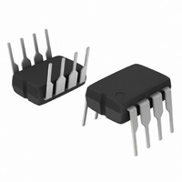
IC CTLR CURRENT MODE 8-DIP
Manufacturer
ON Semiconductor
Type
Pulse Width Modulator Controllerr
Specifications of UC3842BNG
Pwm Type
Current Mode
Number Of Outputs
1
Frequency - Max
275kHz
Duty Cycle
96%
Voltage - Supply
11.5 V ~ 25 V
Buck
No
Boost
Yes
Flyback
Yes
Inverting
No
Doubler
No
Divider
No
Cuk
No
Isolated
Yes
Operating Temperature
0°C ~ 70°C
Package / Case
8-DIP (0.300", 7.62mm)
Frequency-max
275kHz
Duty Cycle (max)
96 % (Typ)
Output Voltage
4.9 V to 5.1 V
Output Current
1000 mA (Max)
Mounting Style
Through Hole
Switching Frequency
500 KHz
Operating Supply Voltage
30 V
Maximum Operating Temperature
70 C
Fall Time
50 ns
Minimum Operating Temperature
0 C
Rise Time
50 ns
Synchronous Pin
No
Topology
Boost or Flyback or Forward
Current, Input Bias
-2 μA
Current, Output
+12 mA (Sink), -1 mA (Source)
Current, Supply
0.3 mA
Frequency, Oscillator
250 kHz
Package Type
PDIP-8
Power Dissipation
1.25 W
Regulation, Line
2 mV
Regulation, Load
3 mV
Regulator Type
DC-DC
Temperature, Operating, Range
0 to +70 °C
Time, Fall
50 ns
Time, Rise
50 ns
Voltage, Gain
3 V/V
Voltage, Input
2.5 V
Voltage, Noise
50 μV
Voltage, Output
5 V
Voltage, Output, High
6.2 V
Voltage, Output, Low
0.8 V
Voltage, Supply
30 V
Voltage, Supply, Rejection Ratio
70 dB
Lead Free Status / RoHS Status
Lead free / RoHS Compliant
Other names
UC3842BNGOS
Available stocks
Company
Part Number
Manufacturer
Quantity
Price

Part Number:
UC3842BNG
Manufacturer:
ON/安森美
Quantity:
20 000


PIN FUNCTION DESCRIPTION
8−Pin
- 2.0
-1.0
3.0
2.0
1.0
1
2
3
4
5
6
7
8
0
0
0
Ä Ä Ä
14−Pin
2,4,6,1
V
Ä Ä Ä Ä
Ä Ä Ä Ä
10
12
14
11
Figure 16. Output Cross Conduction
Figure 14. Output Saturation Voltage
CC
1
3
5
7
8
9
3
T
A
Ä Ä Ä
Ä Ä Ä
T
= 25°C
A
200
= - 55°C
I
O
Compensation
, OUTPUT LOAD CURRENT (mA)
versus Load Current
Feedback
Function
Voltage
Current
Ground
Output
Sense
Power
R
Ä Ä Ä Ä Ä
Ä Ä Ä Ä Ä
Ä Ä Ä Ä
Ä Ä Ä Ä
Ä Ä Ä Ä
Ä Ä Ä Ä
GND
GND
V
V
NC
T
V
CC
/C
ref
Source Saturation
(Load to Ground)
C
Sink Saturation
(Load to V
T
T
100 ns/DIV
A
= - 55°C
400
CC
This pin is the Error Amplifier output and is made available for loop compensation.
This is the inverting input of the Error Amplifier. It is normally connected to the switching power
supply output through a resistor divider.
A voltage proportional to inductor current is connected to this input. The PWM uses this
information to terminate the output switch conduction.
The Oscillator frequency and maximum Output duty cycle are programmed by connecting resistor
R
This pin is the combined control circuitry and power ground.
This output directly drives the gate of a power MOSFET. Peak currents up to 1.0 A are sourced
and sunk by this pin.
This pin is the positive supply of the control IC.
This is the reference output. It provides charging current for capacitor C
This pin is a separate power ground return that is connected back to the power source. It is used
to reduce the effects of switching transient noise on the control circuitry.
The Output high state (V
source connection, it can reduce the effects of switching transient noise on the control circuitry.
This pin is the control circuitry ground return and is connected back to the power source ground.
No connection. These pins are not internally connected.
)
T
to V
Ä Ä Ä Ä Ä
Ä Ä Ä Ä Ä
Ä Ä Ä Ä Ä
80 ms Pulsed Load
ref
Ä Ä Ä
Ä Ä Ä
Ä Ä
GND
600
120 Hz Rate
T
and capacitor C
V
V
C
T
A
CC
A
CC
L
= 25°C
= 25°C
= 15 pF
= 15 V
= 30 V
http://onsemi.com
800
OH
T
) is set by the voltage applied to this pin. With a separate power
to ground. Operation to 500 kHz is possible.
7
90%
10%
25
20
15
10
5
0
0
Figure 17. Supply Current versus Supply Voltage
Description
Figure 15. Output Waveform
10
V
CC
, SUPPLY VOLTAGE (V)
50 ns/DIV
20
T
through resistor R
Ä Ä Ä Ä
Ä Ä Ä Ä
Ä Ä Ä Ä
Ä Ä Ä Ä
R
C
V
I
T
Sense
A
T
T
FB
= 25°C
= 10 k
= 3.3 nF
= 0 V
30
V
C
T
= 0 V
A
CC
L
= 25°C
= 1.0 nF
= 15 V
T
.
40
Related parts for UC3842BNG
Image
Part Number
Description
Manufacturer
Datasheet
Request
R

Part Number:
Description:
ON Semiconductor [VOLTAGE REGULATOR]
Manufacturer:
ON Semiconductor
Datasheet:
Part Number:
Description:
357-036-542-201 CARDEDGE 36POS DL .156 BLK LOPRO
Manufacturer:
ON Semiconductor
Datasheet:
Part Number:
Description:
357-036-542-201 CARDEDGE 36POS DL .156 BLK LOPRO
Manufacturer:
ON Semiconductor
Datasheet:
Part Number:
Description:
357-036-542-201 CARDEDGE 36POS DL .156 BLK LOPRO
Manufacturer:
ON Semiconductor
Datasheet:
Part Number:
Description:
357-036-542-201 CARDEDGE 36POS DL .156 BLK LOPRO
Manufacturer:
ON Semiconductor
Datasheet:
Part Number:
Description:
357-036-542-201 CARDEDGE 36POS DL .156 BLK LOPRO
Manufacturer:
ON Semiconductor
Datasheet:
Part Number:
Description:
357-036-542-201 CARDEDGE 36POS DL .156 BLK LOPRO
Manufacturer:
ON Semiconductor
Datasheet:
Part Number:
Description:
357-036-542-201 CARDEDGE 36POS DL .156 BLK LOPRO
Manufacturer:
ON Semiconductor
Datasheet:
Part Number:
Description:
357-036-542-201 CARDEDGE 36POS DL .156 BLK LOPRO
Manufacturer:
ON Semiconductor
Datasheet:
Part Number:
Description:
357-036-542-201 CARDEDGE 36POS DL .156 BLK LOPRO
Manufacturer:
ON Semiconductor
Datasheet:
Part Number:
Description:
357-036-542-201 CARDEDGE 36POS DL .156 BLK LOPRO
Manufacturer:
ON Semiconductor
Datasheet:
Part Number:
Description:
Manufacturer:
ON Semiconductor
Datasheet:
Part Number:
Description:
Manufacturer:
ON Semiconductor
Datasheet:
Part Number:
Description:
Manufacturer:
ON Semiconductor
Datasheet: