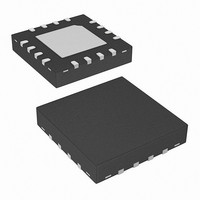
ISL6269IRZ Intersil, ISL6269IRZ Datasheet - Page 10

ISL6269IRZ
Manufacturer Part Number
ISL6269IRZ
Description
IC PWM CTRLR SYNC BUCK 16-QFN
Manufacturer
Intersil
Datasheet
1.ISL6269CRZ.pdf
(14 pages)
Specifications of ISL6269IRZ
Pwm Type
Controller
Number Of Outputs
1
Frequency - Max
600kHz
Voltage - Supply
7 V ~ 25 V
Buck
Yes
Boost
No
Flyback
No
Inverting
No
Doubler
No
Divider
No
Cuk
No
Isolated
No
Operating Temperature
-40°C ~ 100°C
Package / Case
16-VQFN Exposed Pad, 16-HVQFN, 16-SQFN, 16-DHVQFN
Frequency-max
600kHz
Lead Free Status / RoHS Status
Lead free / RoHS Compliant
Duty Cycle
-
Programming the Output Voltage
When the converter is in regulation there will be 600mV from
the FB pin to the GND pin. Connect a two-resistor voltage
divider across the VO pin and the GND pin with the output
node connected to the FB pin. Scale the voltage-divider
network such that the FB pin is 600mV with respect to the
GND pin when the converter is regulating at the desired
output voltage. The output voltage can be programmed from
600mV to 3.3V.
Programming the output voltage is written as:
Where:
Beginning with R
R
Programming the PWM Switching Frequency
The ISL6269 does not use a clock signal to produce PWM.
The PWM switching frequency f
resistor R
GND pin. The approximate PWM switching frequency is
written as:
Estimating the value of R
Where:
It is recommended that whenever the control loop
compensation network is modified, f
for the correct frequency and if necessary, adjust R
Compensation Design
The LC output filter has a double pole at its resonant frequency
that causes the phase to abruptly roll downward. The R
modulator used in the ISL6269 makes the LC output filter
resemble a first order system in which the closed loop stability
can be achieved with a Type II compensation network.
V
R
f
R
SW
BOTTOM
REF
BOTTOM
FSET
- V
- V
- R
- R
- f
- R
- K = 75 x 10
between the FB pin and the GND pin
from the FB pin to the VO pin. In addition to setting the
output voltage, this resistor is part of the loop
compensation network
connects from the FB pin to the GND pin
=
SW
OUT
REF
TOP
BOTTOM
FSET
=
-------------------------- -
K R
=
V
⋅
is the PWM switching frequency
FSET
----------------- -
K f
OUT
is the voltage that the converter regulates to
is the voltage-programming resistor that connects
is the desired output voltage of the converter
is written as:
=
1
FSET
•
is the f
1
SW
------------------------------------ -
V
V
•
OUT
REF
-------------------------------------------------- -
R
is the voltage-programming resistor that
that is connected from the FSET pin to the
-12
TOP
TOP
SW
R
•
–
R
BOTTOM
V
+
TOP
between 1kΩ to 5kΩ, calculating
REF
programming resistor
R
BOTTOM
FSET
10
is written as:
SW
is programmed by the
SW
should be checked
FSET
3
(EQ. 5)
(EQ. 6)
(EQ. 7)
(EQ. 8)
.
ISL6269
Your local Intersil representative can provide a PC-based
tool that can be used to calculate compensation network
component values and help simulate the loop frequency
response. The compensation network consists of the internal
error amplifier of the ISL6269 and the external components R1,
R2, C1, and C2 as well as the frequency setting components
R
General Application Design Guide
This design guide is intended to provide a high-level
explanation of the steps necessary to create a single-phase
power converter. It is assumed that the reader is familiar with
many of the basic skills and techniques referenced below. In
FSET
COMP
FIGURE 6. COMPENSATION REFERENCE CIRCUIT
, and C
R
GATE DRIVERS
3
ISL6269
MODULATOR
R2
REF
EA
FSET,
PHASE
+
-
FSET
C2
GND
VIN
VO
UG
LG
FB
are identified in the schematic Figure 6.
C1
R
FSET
Q
Q
HIGH_SIDE
LOW_SIDE
L
VOUT
R1
OUT
VIN
C
C
DCR
OUT
ESR
C
FSET
June 25, 2009
FN9177.3


