SC412AMLTRT Semtech, SC412AMLTRT Datasheet
SC412AMLTRT
Specifications of SC412AMLTRT
Available stocks


Related parts for SC412AMLTRT


SC412AMLTRT Summary of contents
Page 1
... Non-Overlapping Gate Drive with SmartDrive™ High Effi ciency > 90% Fully WEEE and RoHS Compliant † Patent pending Applications Notebook and Sub-Notebook Voltage Controllers Tablet PCs Embedded Applications D1 RLIM BST 3 VCC VCC Q2 SC412A SC412A or Resistor DS(ON) † VCC PGOOD PGOOD 10 VOUT VOUT www.semtech.com ...
Page 2
... Parameter Input Supplies VBAT Input Voltage VCC Shutdown Current VCC Operating Current Controller FB On-Time Threshold Regulation Line Regulation Error Typical Application Circuit Load Regulation Error Typical Application Circuit © 2006 Semtech Corp. Symbol θ ( 0.1% resistor dividers 5.0V, unless otherwise noted. o ...
Page 3
... Over-Voltage Fault Over-Voltage Fault Delay (1) Over-Voltage Fault Threshold VCCA Under-Voltage Conditions = Falling Edge (UVLO) Over-Temperature Shutdown (1) Logic Inputs/Outputs Logic Input Hgh Voltage Logic Input Low Voltage © 2006 Semtech Corp. Conditions Min V = 1.1V OUT V < V +0.2 BAT OUT < On-Time Threshold OUT ...
Page 4
... Guaranteed by design. (2) Semtech’s SmartDriver™ FET drive fi rst pulls DH high with a pull-up resistance of 10Ω (typical) until LX = 1.5V (typical). At this point, an additional pull-up device is activated, reducing the resistance to 2Ω (typical). This negates the need for an external gate or boost resistor. © ...
Page 5
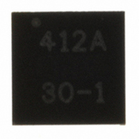
... Marking for the 3 x 3mm MLPQ 16 Lead Package nnnn = Part Number (example: 412A) yyww = Date Code (example: 0652) xxxx = Semtech Lot No. (example: E901) © 2006 Semtech Corp. Ordering Information SC412AMLTRT EN 12 Notes: PGOOD 1) Available in tape and reel packaging only. A reel contains 3000 11 devices ...
Page 6
... Not connected internally — leave unconnected or connect to GND 16 DH Gate drive output for the high-side external FET Thermal pad for heatsinking purposes — not connected internally — connect to system T PAD ground through preferably one large via or multiple smaller vias © 2006 Semtech Corp. 6 SC412A www.semtech.com ...
Page 7
... NOT RECOMMENDED FOR NEW DESIGN POWER MANAGEMENT Block Diagram +5V BST VBAT DH VOUT LX DL ILIM © 2006 Semtech Corp. Enable Power Good EN Control and Status DRV TON Generator Gate Drive Control DRV Zero Cross/Negative I-limit Detect Valley I-Limit Block Diagram 7 SC412A +5V VCC ...
Page 8
... ESR Figure 1. © 2006 Semtech Corp. On-Time One-Shot (T The internal on-time one-shot comparator has two inputs. One input looks at the output voltage via the VOUT pin, while the other input samples the input voltage via the LX pin and converts proportional current which charges an internal on-time capacitor ...
Page 9
... VOUT back to VBAT and prevents a hard OVP shutdown, and also minimizes operating power by avoiding continuous conduction-mode operation. © 2006 Semtech Corp. Current Limit Circuit Current limiting can be accomplished in two ways. The RD- SON of the lower MOSFET can be used as a current sensing element sense resistor at the lower MOSFET source can be used if greater accuracy is needed ...
Page 10
... BST DH LX ILIM VDD Q2 DL GND SC412A R1 R4 Figure 5. © 2006 Semtech Corp. = The following over-current equation can be used for both ILIM RDS or resistive sensing. For RDS ON RDS rating is used for the value Power Good Output VOUT The power good (PGD) output is an open-drain output which requires a pull-up resistor ...
Page 11
... The high-side MOSFET conducts and causes LX to rise; when LX reaches 1.5volts, the DH drive resistance is reduced to 2 ohms to provide fast switching and reduce switching loss. © 2006 Semtech Corp. Design Procedure Prior to designing a switch mode supply, the input voltage, load current, switching frequency and inductor ripple cur- rent must be specifi ...
Page 12
... BAT OUT ON RIPPLE I = (10 - 1.15) • 329 nsec / 0.7μH = 4.16A RIPPLE_VBATMIN © 2006 Semtech Corp. Capacitor Selection The output capacitors are chosen based on required ESR and capacitance. The ESR requirement is driven by the / output ripple requirement and the DC tolerance. The BAT output voltage has a DC value that is equal to the valley of the output ripple, plus 1/2 of the peak-to-peak ripple ...
Page 13
... Unstable operation shows up in two related but distinctly different ways: double-pulsing and fast-feedback loop instability. double-pulsing occurs due to switching noise © 2006 Semtech Corp. seen at the FB input or because the ESR is too low, caus- ing insuffi cient voltage ramp in the FB signal. This causes the error amplifi ...
Page 14
... The error comparator offset is trimmed so that it trips when the feedback pin is 0.75V, 1%. © 2006 Semtech Corp. The on-time pulse in the SC412A is calculated to give a pseudo-fi xed frequency of 325kHz. Nevertheless, some frequency variation with line and load is expected. This variation changes the output ripple voltage ...
Page 15
... C R2 OUT Figure 7. © 2006 Semtech Corp also possible to lower the frequency using a resistive divider to the 5V bias supply, see Figure 3. This raises the voltage at the VOUT pin which will increase the on-time. Note that this results in a small leakage path from the 5V supply to the output voltage. The resistor values should be fairly large (> ...
Page 16
... Use multiple vias as required by current handling requirement (and to reduce parasitic) if routed on more than one layer. © 2006 Semtech Corp. For an accurate ILIM current sense connection, connect the ILIM trace to the current sense element (MOSFET or resistor) directly at the pin of the element, and route that trace over to the ILIM resistor on another layer if needed. The layout can be generally considered in two parts ...
Page 17
... Route the VOUT feedback trace in a “quiet” layer, away from noise sources. © 2006 Semtech Corp. 2) Route DL, DH and LX (low side FET gate drive, high side FET gate drive and phase node) to the chip using wide traces, with multiple vias if using more than one layer. ...
Page 18
... VBAT (V) Load Regulation 1.13 1.12 19V 1.11 1.10 10V 1.09 1.08 1. Load (A) Note: See Reference schematic on Page 20. © 2006 Semtech Corp. 1000 900 800 700 600 5V 500 400 300 200 100 15 20 95% 1.5V 90% 1.25V 85% 80% 0.75V 75 1.13 1 ...
Page 19
... NOT RECOMMENDED FOR NEW DESIGN POWER MANAGEMENT Typical Characteristics (continued) Startup 1.15V 19VBAT No load Load Transient Response 0A to 20A Note: See Reference schematic on Page 20 © 2006 Semtech Corp. Startup 1.15V 19VBAT 20A load Load Transient Response 20A SC412A www.semtech.com ...
Page 20
... L1 + C5 1UF MBRS140L *330uF/6mohm Bill of Materials Component Value 10uF, 25V C1, C2, C3 C5, C5 330uF/6mohm/2V L1 0.7uH, 24A Q1 10mohm/30V Q2 3.5mohm/30V D1 200mA/30V D2 1A/40V © 2006 Semtech Corp. VCC D1 BAT54A 4 R4 10K C4 100NF 1 LX VCC 2 BST D 3 VCC PAD RJK0302DP C8 1UF Reference Design 1.15V 20A ...
Page 21
... NOT RECOMMENDED FOR NEW DESIGN POWER MANAGEMENT Outline Drawing - MLPQ-16 3x3 A PIN 1 INDICATOR (LASER MARK) A aaa NOTES: 1. CONTROLLING DIMENSIONS ARE IN MILLIMETERS (ANGLES IN DEGREES). 2. COPLANARITY APPLIES TO THE EXPOSED PAD AS WELL AS THE TERMINALS. 3. DAP IS 1.90 x 1.90mm. © 2006 Semtech Corp DIM aaa bbb SEATING ...
Page 22
... COMPANY'S MANUFACTURING GUIDELINES ARE MET. THERMAL VIAS IN THE LAND PATTERN OF THE EXPOSED PAD 2. SHALL BE CONNECTED TO A SYSTEM GROUND PLANE. FAILURE MAY COMPROMISE THE THERMAL AND/OR FUNCTIONAL PERFORMANCE OF THE DEVICE. Contact Information Phone: (805) 498-2111 Fax: (805) 498-3804 © 2006 Semtech Corp. DIM ...