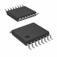
LM5032MTC/NOPB National Semiconductor, LM5032MTC/NOPB Datasheet

LM5032MTC/NOPB
Specifications of LM5032MTC/NOPB
*LM5032MTC/NOPB
LM5032MTC
Available stocks
Related parts for LM5032MTC/NOPB
LM5032MTC/NOPB Summary of contents
Page 1
... MHz capable oscil- lator with synchronization capability. Typical Application Circuit Dual Interleaved Regulators with Independent Outputs © 2005 National Semiconductor Corporation Features n Two independent PWM current mode controllers n Integrated high voltage startup regulator n Compound 2.5A main output gate drivers ...
Page 2
Connection Diagram Ordering Information Order Number Package Type LM5032MTC TSSOP-16 LM5032MTCX TSSOP-16 Pin Description PIN NAME DESCRIPTION 1 VIN Input Supply 2 COMP1 PWM Control, Controller 1 3 CS1 Current Sense Input, Controller 1 4 SS1 Soft-start, Controller 1 5 ...
Page 3
Pin Description (Continued) PIN NAME DESCRIPTION 8 GND1 Ground, Controller 1 9 GND2 Ground, Controller 2 10 OUT2 Main Gate Driver, Controller 2 11 RES Hiccup mode restart adjust 12 SS2 Soft-start, Controller 2 13 CS2 Current Sense Input, Controller ...
Page 4
Block Diagram www.national.com FIGURE 1. Detailed Block Diagram 4 20135003 ...
Page 5
... Absolute Maximum Ratings If Military/Aerospace specified devices are required, please contact the National Semiconductor Sales Office/ Distributors for availability and specifications. VIN to GND VCC to GND RT/SYNC, RES and DCL to GND CS Pins to GND All other inputs to GND ESD Rating (Note 5) Human Body Model ...
Page 6
Electrical Characteristics Specifications with standard typeface are for T Temperature range. VIN = 48V, VCC = 10V externally applied, R stated (Note 3) and (Note 4). Symbol Parameter Oscillator (RT/SYNC Pin) F Frequency 1 (at OUT1, S1 OUT2) F Frequency ...
Page 7
... For guaranteed specifications and test conditions, see the Electrical Characteristics. Note 2: For detailed information on soldering plastic TSSOP packages, refer to the Packaging Data Book available from National Semiconductor Corporation. Note 3: All limits are guaranteed. All electrical characteristics having room temperature limits are tested during production with T guaranteed by correlating the electrical characteristics to process and temperature variations and applying statistical process control. Note 4: Typical specifications represent the most likely parametric norm at 25˚ ...
Page 8
Typical Performance Characteristics FIGURE VIN IN FIGURE VIN IN www.national.com 20135006 FIGURE 5. I 20135007 FIGURE 6. VCC vs VIN 8 20135008 vs Externally Applied VCC CC 20135009 ...
Page 9
Typical Performance Characteristics (Continued) FIGURE 7. VCC vs I (Externally Loaded) CC FIGURE 8. Oscillator Frequency vs R FIGURE 9. User Defined Maximum Duty Cycle vs. R 20135010 FIGURE 10. Maximum Duty Cycle vs. UVLO Voltage 20135011 Resistor T 9 ...
Page 10
Typical Performance Characteristics (Continued) FIGURE 11. Maximum Duty Cycle vs. VIN (Figure 25) FIGURE 12. Frequency vs. Temperature www.national.com FIGURE 13. Soft-start Pin Current vs. Temperature 20135014 FIGURE 14. Current Limit Threshold at CS1, CS2 vs. 20135016 10 20135018 20135019 ...
Page 11
Functional Description The LM5032 contains all the features necessary to imple- ment two independently regulated current mode dc/dc con- verters single high current converter comprised of two parallel interleaved channels using the Forward converter topology. The two controllers ...
Page 12
Oscillator (Continued) age at the R /SYNC pin is internally regulated at 2.0V. The T R resistor should be located as close as possible to the T LM5032 with short direct connections to the pins. The LM5032 can be synchronized ...
Page 13
Hiccup Mode Current Limit Restart (Continued) The 10 µA discharge current source at RES is enabled pulling the RES pin to ground. b) Current limit repeatedly detected at both CS inputs: The 20 µA current source at RES is enabled ...
Page 14
Hiccup Mode Current Limit Restart Soft-start Each soft-start circuit allows the corresponding regulator to gradually reach a steady state operating point, thereby re- ducing startup current surges and output overshoot. Upon turn-on, both SS pins are internally held at ground. ...
Page 15
Output Duty Cycle (Continued) driver pulsewidth is equal to the least of these four pulses. Whichever input of the AND gate transitions high-to-low first terminates the output driver’s on-time. Driver Outputs OUT1, the primary switch driver for Controller 1 is ...
Page 16
Applications Information VIN The voltage applied to the VIN pin, normally the same as the system voltage applied to the power transformer’s primary (V ), can vary in the range 100V with transient PWR capability to 105V. ...
Page 17
Applications Information FIGURE 24. Shutdown Control VCC The capacitor at VCC provides not only regulator noise filtering and stability, but also prevents VCC from dropping to the lower under-voltage threshold level (UVT = 6.2V) when the output drivers source current ...
Page 18
Applications Information FIGURE 26. Current Sense Using a Current Sense Transformer FIGURE 27. Current Sense Using a Source Sense Resistor (R1) HICCUP MODE CURRENT LIMIT RESTART This circuit’s operation is described in the Functional De- scription. Also see Figures 17 ...
Page 19
Applications Information With a 0.1 µF capacitor at SS )150 ms. Experimentation with the startup sequence and over-current restart condition is usually necessary to determine the ap- propriate value for the SS capacitors. To shutdown one regulator without ...
Page 20
Applications Information www.national.com (Continued) 20135042 FIGURE 30. Total Board Efficiency 20 ...
Page 21
21 www.national.com ...
Page 22
... BANNED SUBSTANCE COMPLIANCE National Semiconductor manufactures products and uses packing materials that meet the provisions of the Customer Products Stewardship Specification (CSP-9-111C2) and the Banned Substances and Materials of Interest Specification (CSP-9-111S2) and contain no ‘‘Banned Substances’’ as defined in CSP-9-111S2. ...


