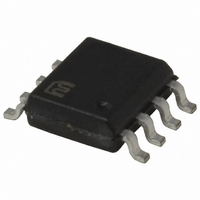
MIC5156-5.0BM Micrel Inc, MIC5156-5.0BM Datasheet - Page 7

MIC5156-5.0BM
Manufacturer Part Number
MIC5156-5.0BM
Description
IC CTRLR LDO REG 5.0V 8-SOIC
Manufacturer
Micrel Inc
Type
Positive Fixedr
Datasheet
1.MIC5156YM.pdf
(13 pages)
Specifications of MIC5156-5.0BM
Number Of Outputs
1
Voltage - Output
5V
Current - Supply
2.7mA
Voltage - Input
3 ~ 36 V
Operating Temperature
-40°C ~ 85°C
Package / Case
8-SOIC (3.9mm Width)
Lead Free Status / RoHS Status
Contains lead / RoHS non-compliant
Block Diagram MIC5158
Functional Description
A Super LDO Regulator is a complete regulator built around
Micrel’s Super LDO Regulator Controller.
Refer to Block Diagrams MIC5156, MIC5157, and
MIC5158.
Version Differences
The MIC5156 requires an external voltage for MOSFET gate
drive and is available in 3.3V fixed output, 5V fixed output, or
adjustable output versions. With 8-pins, the MIC5156 is the
smallest of the Super LDO Regulator Controllers.
The MIC5157 and MIC5158 each have an internal charge
pump which provides MOSFET gate drive voltage. The
MIC5157 has a selectable fixed output of 3.3V, 5V, or 12V.
The MIC5158 may be configured for a fixed 5V or adjustable
output.
Enable (EN)
With at least 3.0V on V
the controller in shutdown mode. A TTL high on EN enables
the internal bias circuit which powers all internal circuitry. EN
must be pulled high if unused. The voltage applied to EN may
be as high as 36V.
The controller draws less than 1µA in shutdown mode.
Gate Enhancement
The Super LDO Regulator Controller manages the gate-
August 2005
MIC5156/5157/5158
F L A G
DD
, applying a TTL low to EN places
Oscillator
Adjustable Power Supply, 3.6V Configuration
C1+ C1– C2+ C2–
V
Comparator
0.1µF
Block Diagram with External Components
OU T
Charge Pump
Reference
C1
Bandgap
1.235V
75mV
Tripler
0.1µF
Error
Amp
C2
V
C P
7
C3
Clamp
to-source enhancement voltage for an external N-channel
MOSFET (regulator pass element) placed between the supply
and the load. The gate-to-source voltage may vary from 1V
to 16V depending upon the supply and load conditions.
Because the source voltage (output) approaches the drain
voltage (input) when the regulator is in dropout and the
MOSFET is fully enhanced, an additional higher supply
voltage is required to produce the necessary gate-to-source
enhancement. This higher gate drive voltage is provided by
an external gate drive supply (MIC5156) or by an internal
charge pump (MIC5157 and MIC5158).
Gate Drive Supply Voltage (MIC5156 only)
The gate drive supply voltage must not be more than 14V
above the supply voltage (V
necessary gate drive supply voltage is:
where:
The error amplifier uses the gate drive supply voltage to drive
the gate of the external MOSFET. The error amplifier output
can swing to within 1V of V
1µF
V
C P
V
V
V
V
I
Comparator
LIMIT
P
P
OUT
GS
MOSFET gate enhancement
= V
= gate drive supply voltage
= gate-to-source voltage for full
= regulator output voltage
32k
10k
Internal
Bias
OUT
internal blocks
+5V Input
V
to all
35mV
DD
+ V
16.6V
GS
+ 1
E N
D (Drain)
[ I
G (Gate)
S (Source)
5V
F B
GND
E A
LIMIT
P
Enable
Shutdown
.
P
]
– V
19.1k
10.0k
DD
C
R
3mΩ
Q1
IRFZ44
L
S
< 14V). The minimum
MIC5156/5157/5158
Regulated
+3.6V Output
Micrel, Inc.


