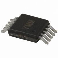
MIC5190BMM Micrel Inc, MIC5190BMM Datasheet - Page 7

MIC5190BMM
Manufacturer Part Number
MIC5190BMM
Description
IC CTRLR LDO/FILTER HS 10MSOP
Manufacturer
Micrel Inc
Type
Positive Adjustabler
Datasheet
1.MIC5190YMM.pdf
(13 pages)
Specifications of MIC5190BMM
Number Of Outputs
1
Voltage - Output
Adjustable
Current - Supply
15mA
Voltage - Input
0.9 ~ 5.5 V
Operating Temperature
-40°C ~ 125°C
Package / Case
10-MSOP, Micro10™, 10-uMAX, 10-uSOP
Lead Free Status / RoHS Status
Contains lead / RoHS non-compliant
December 2005
Applications Information
Designing with the MIC5190
Anatomy of a transient response
The measure of a regulator is how accurately and effectively
it can maintain a set output voltage, regardless of the load's
power demands. One measure of regulator response is the
load step. The load step gauges how the regulator responds
to a change in load current. Figure 2 is a look at the transient
response to a load step.
At the start of a circuit's power demand, the output voltage is
regulated to its set point, while the load current runs at a
constant rate. For many different reasons, a load may ask for
more current without warning. When this happens, the regu-
lator needs some time to determine the output voltage drop.
This is determined by the speed of the control loop. So, until
enough time has elapsed, the control loop is oblivious to the
voltage change. The output capacitor must bear the burden
of maintaining the output voltage.
Since this is a sudden change in voltage, the capacitor will try
to maintain voltage by discharging current to the output. The
first voltage drop is due to the output capacitor's ESL (equiva-
lent series inductance). The ESL will resist a sudden change
in current from the capacitor and drop the voltage quickly. The
amount of voltage drop during this time will be proportional to
the output capacitor's ESL and the speed at which the load
steps. Slower load current transients will reduce this effect.
Placing multiple small capacitors with low ESL in parallel can
help reduce the total ESL and reduce voltage droop during
high speed transients. For high speed transients, the greatest
voltage deviation will generally be caused by output capacitor
ESL and parasitic inductance.
After the current has overcome the effects of the ESL, the
output voltage will begin to drop proportionally to time and
inversely proportional to output capacitance.
MIC5190
V
V
V L
Figure 2. Typical Transient Response
L
L
dt
di
V
dt
di
L
dt
di
Time
dt
di
V =
BW
1
C
1
idt
Output voltage vs. time
directly proportional to
gain vs. frequency.
during recovery is
7
Output voltage variation will depend on two factors: loop
bandwidth and output capacitance. The output capacitance
will determine how far the voltage will fall over a given time.
With more capacitance, the drop in voltage will fall at a
decreased rate. This is the reason that more capacitance
provides a better transient response for the same given
bandwidth.
The time it takes for the regulator to respond is directly
proportional to its bandwidth gain. Higher bandwidth control
loops respond quicker causing a reduced drop on the supply
for the same amount of capacitance.
Final recovery back to the regulated voltage is the final phase
of transient response and the most important factors are gain
and time. Higher gain at higher frequency will get the output
voltage closer to its regulation point quicker. The final settling
point will be determined by the load regulation, which is
proportional to DC (0Hz) gain and the associated loss terms.
There are other factors that contribute to large signal tran-
sient response, such as source impedance, phase margin,
and PSRR. For example, if the input voltage drops due to
source impedance during a load transient, this will contribute
to the output voltage deviation by filtering through to the
output reduced by the loops PSRR at the frequency of the
voltage transient. It is straightforward: good input capaci-
tance reduces the source impedance at high frequencies.
Having between 35 and 45 of phase margin will help speed
up the recovery time. This is caused by the initial overshoot
in response to the loop sensing a low voltage.
Compensation
The MIC5190 has the ability to externally control gain and
bandwidth. This allows the MIC5190 design to be individually
tailored for different applications.
In designing the MIC5190, it is important to maintain ad-
equate phase margin. This is generally achieved by having
the gain cross the 0dB point with a single pole 20dB/decade
roll-off. The compensation pin is configured as Figure 3
demonstrates.
V
V
V
C
1
Figure 3. Internal Compensation
C
1
1
idt
C
idt
idt
Error Amplifier
External
20pF
3.42M
Internal
Comp
Driver
M9999-120105
Micrel


