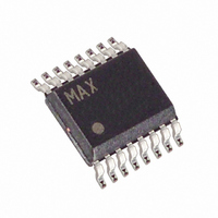
MAX8563EEE+T Maxim Integrated Products, MAX8563EEE+T Datasheet - Page 11

MAX8563EEE+T
Manufacturer Part Number
MAX8563EEE+T
Description
IC CNTRLR N-FET 16-QSOP
Manufacturer
Maxim Integrated Products
Type
Positive Adjustabler
Datasheet
1.MAX8564AEUB.pdf
(15 pages)
Specifications of MAX8563EEE+T
Number Of Outputs
3
Voltage - Output
0.5 ~ 1.8 V, 0.5 ~ 3.3 V
Current - Supply
930µA
Voltage - Input
5V, 12V
Operating Temperature
-40°C ~ 85°C
Package / Case
16-QSOP
Lead Free Status / RoHS Status
Lead free / RoHS Compliant
To set the output voltage to 0.5V, disconnect R
FB_ and connect it to OUT_; this change maintains the
minimum load requirement on the output. In this case,
R
The input filter capacitor aids in providing low input
impedance to the regulator and also reduces peak cur-
rents drawn from the power source during transient
conditions. Use a minimum 2.2µF ceramic capacitor
from IN_ (drain of the external pass n-MOSFET) to GND
(see Figures 1 and 2). If large line transients or load
transients are expected, increase the input capaci-
tance to help minimize output voltage changes.
The output filter capacitor and its equivalent series
resistance (ESR) contribute to the stability of the regula-
tor (see the Stability Compensation section) and affect
the load-transient response. If large step loads (no load
to full load) are expected, and a very fast response
(less than a few microseconds) is required, use a
100µF, 18m
larger capacitance is desired, keep the capacitance
ESR product (C
If the application expects smaller load steps (less than
50% of full load), then use a 6.8µF ceramic capacitor or
larger per ampere of maximum output current. This
option reduces the size and cost of the regulator circuit.
Note that some ceramic dielectrics exhibit large capaci-
tance variation with temperature. Use X7R or X5R
dielectrics to ensure sufficient capacitance at all operat-
ing temperatures. Tantalum and aluminum capacitors
are not recommended.
The MAX8563/MAX8564/MAX8564A use an n-channel
MOSFET as the series pass transistor instead of a p-
channel MOSFET to reduce cost. The selected MOS-
FET must have a gate threshold voltage that meets the
following criteria:
where V
is the maximum gate voltage required to yield the on-
resistance (R
data sheet. R
R
±1%, Ultra-Low Output Voltage, Dual and Triple
A
A
can vary from 1k to 10k .
Input and Output Capacitor Selection
R
DD
B
is the controller bias voltage, and V
DS_ON
DS_ON
POSCAP for the output capacitor. If a
OUT
V
V
GS_MAX
V
OUT
______________________________________________________________________________________
FB
x R
) specified by the manufacturer’s
multiplied by the maximum output
Power MOSFET Selection
ESR
1
) in the 1µs to 5µs range.
V
DD
- V
R
B
OUT_
2
V
OUT
GS_MAX
B
from
1
Linear n-FET Controllers
current (load current) is the maximum voltage dropout
across the MOSFET, V
meets the condition below to avoid entering dropout,
where output voltage starts to decrease and any ripple
on the input also passes through to the output:
where V
of the MOSFET. V
coefficient; therefore, the value of V
operating junction temperature should be used.
For thermal management, the maximum power dissipa-
tion in the MOSFET is calculated by:
The MOSFET is typically in an SMT package. Refer to
the MOSFET data sheet for the PC board area needed
to meet the maximum operating junction temperature
required.
Connect a resistor, R
from the DRV_ pin to GND. The values of the compen-
sation network depend upon the external MOSFET
characteristics, the output current range, and the pro-
grammed output voltage. The following parameters are
needed from the MOSFET data sheet: the input capaci-
tance (C
ductance (g
measured (I
the FET at the maximum load current (I
Figure 5. Adjustable Output Voltage
IN_MIN
ISS
P
D
g
at V
DFS
C MAX
FS
= (V
V
(
is the minimum input voltage at the drain
IN_MIN
), and the current at which g
DS
). Calculate the transconductance of
MAX8564A
IN_MAX
MAX8563
MAX8564
DS
)
= 1V), the typical forward transcon-
_
C
DS
> V
MIN
, and a capacitor, C
g
FS
_
Stability Compensation
FB_
- V
DS
MIN
has a positive temperature
OUT
_
MIN
. Make sure that V
) x I
I
OUT MAX
+ V
DS
R
R
I
OUT_MAX
A
B
DFS
_
OUT
OUT_
_
MIN
OUT_MAX
at the highest
C
, in series
):
FS
DS
_
was
MIN
11


