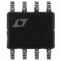
LT1573CS8 Linear Technology, LT1573CS8 Datasheet - Page 5

LT1573CS8
Manufacturer Part Number
LT1573CS8
Description
IC LDO REGULATOR DVR ADJ 8-SOIC
Manufacturer
Linear Technology
Type
Positive Adjustabler
Datasheet
1.LT1573CS8.pdf
(16 pages)
Specifications of LT1573CS8
Number Of Outputs
1
Voltage - Output
1.27 ~ 6.8 V
Current - Supply
1.7mA
Voltage - Input
2.8 ~ 10 V
Operating Temperature
0°C ~ 125°C
Package / Case
8-SOIC (3.9mm Width)
Lead Free Status / RoHS Status
Contains lead / RoHS non-compliant
Available stocks
Company
Part Number
Manufacturer
Quantity
Price
Company:
Part Number:
LT1573CS8
Manufacturer:
Linear Technology
Quantity:
135
Company:
Part Number:
LT1573CS8
Manufacturer:
LT
Quantity:
2 368
Part Number:
LT1573CS8
Manufacturer:
LT/凌特
Quantity:
20 000
Company:
Part Number:
LT1573CS8#PBF
Manufacturer:
LT
Quantity:
1 604
Part Number:
LT1573CS8#PBF
Manufacturer:
LINEAR/凌特
Quantity:
20 000
Company:
Part Number:
LT1573CS8#TR
Manufacturer:
NS
Quantity:
86
Company:
Part Number:
LT1573CS8#TRPBF
Manufacturer:
LINEAR
Quantity:
8 031
Part Number:
LT1573CS8#TRPBF
Manufacturer:
LINEAR/凌特
Quantity:
20 000
Part Number:
LT1573CS8-2.5
Manufacturer:
LINEAR/凌特
Quantity:
20 000
Part Number:
LT1573CS8-2.5#PBF
Manufacturer:
LINEAR/凌特
Quantity:
20 000
PI FU CTIO S
FB (Pin 1): The feedback pin is the inverting input of the
error amplifier. The noninverting input of the error ampli-
fier is internally connected to a 1.265V reference. The error
amplifier will servo the drive to the output transistor, Q
in Figure 1, to force the voltage at the feedback pin to be
1.265V. Output voltage is set by a resistor divider as
shown in Figure 1. For adjustable devices an external
resistor divider is used to set the output voltage. For fixed
voltage devices the resistor divider is internal and the top
of the resistor divider is connected to the V
LATCH (Pin 2): The LT1573 provides overcurrent protec-
tion with a timed latch-off circuit. The latch-off time out is
triggered when the DRIVE pin is pulled below the satura-
tion voltage of the drive transistor. The saturation voltage
is a function of the drive current and is equal to approxi-
mately 130mV at 20mA rising to 780mV at 250mA (see
typical performance curves). The time out is set by the
latch charging current and the value of a capacitor con-
nected between the LATCH pin and ground. If the
overcurrent condition persists at the end of the timing
cycle the regulator will latch off until either the latch is reset
or power is cycled off and back on. The latch can be reset
by either pulling the SHDN pin high, pulling current out of
the LATCH pin greater than latching current or grounding
the LATCH pin. Exceeding the thermal limit temperature
will trigger the latch with no timing delay. Under normal
condition, the DC voltage at the LATCH pin is zero. When
the system is latched off, the DC voltage at theLATCH pin
is two V
SHDN (Pin 3): The SHDN pin has two functions. It can be
used to turn off the output voltage by disabling the drive to
the output transistor. It can also be used to reset the
current limit latch. The shutdown/reset functions are
U
BE
U
above ground.
U
OUT
pin.
OUT
activated by applying a voltage > 1.3V to the SHDN pin. The
output voltage will restart as soon as the SHDN pin is
pulled below the shutdown threshold. If the shutdown/
reset function is not used, the pin should be grounded. The
voltage applied to the SHDN pin can be higher than the
input voltage. When the SHDN pin voltage is higher than
2V, the SHDN pin current increases and is limited by an
internal 20k resistor.
GND (Pin 4): Circuit Ground.
DRIVE (Pin 5): The DRIVE pin is connected to the collector
of the main drive transistor of the LT1573. This drive
transistor sinks the base current of the external PNP
output transistor. A resistor is normally inserted between
the base of the external PNP output transistor and the
DRIVE pin. This resistor is sized to allow the LT1573 to
sink the appropriate amount of base current for a given
application and to activate the overcurrent latch in a fault
condition.
V
of the LT1573 including bias, start-up, thermal limit, error
amplifier and all overcurrent latch circuitry.
V
shown in Block Diagram. This pin is normally connected
to the output. The comparator C1 is used to disable the
overcurrent latch during start-up when the output transis-
tor is saturated. For fixed voltage devices the top of the
internal resistor divider that sets the output voltage is
connected to this pin.
COMP (Pin 8): A compensation network is inserted
between the V
transient response. Under normal condition, the DC volt-
age of the COMP pin sits at one V
IN
OUT
(Pin 6): This pin provides power to all internal circuitry
(Pin 7): The V
OUT
OUT
and COMP pins to obtain optimal
pin is the input to comparator C1
BE
above ground.
LT1573
5


