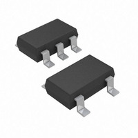
ADR366AUJZ-R2 Analog Devices Inc, ADR366AUJZ-R2 Datasheet - Page 16

ADR366AUJZ-R2
Manufacturer Part Number
ADR366AUJZ-R2
Description
IC VOLT REF 3.3V 25PPM TSOT-23-5
Manufacturer
Analog Devices Inc
Datasheet
1.ADR366AUJZ-R2.pdf
(20 pages)
Specifications of ADR366AUJZ-R2
Temperature Coefficient
25ppm/°C
Reference Type
Series
Voltage - Output
3.3V
Tolerance
±0.25%
Voltage - Input
3.6 ~ 15 V
Number Of Channels
1
Current - Quiescent
190µA
Current - Output
5mA
Operating Temperature
-40°C ~ 125°C
Mounting Type
Surface Mount
Package / Case
TSOT-23-5, TSOT-5, TSOP-5
Topology
Series
Input Voltage
3.6V To 15V
Reference Voltage
3.3V
Reference Voltage Tolerance
8mV
Voltage Reference Case Style
TSOT
No. Of Pins
5
Lead Free Status / RoHS Status
Lead free / RoHS Compliant
Current - Cathode
-
Lead Free Status / Rohs Status
Compliant
Other names
ADR366AUJZ-R2TR
ADR360/ADR361/ADR363/ADR364/ADR365/ADR366
THEORY OF OPERATION
Band gap references are the high performance solution for low
supply voltage and low power voltage reference applications,
and the ADR36x family is no exception. The uniqueness of
these products lies in their architecture. The ideal zero TC band
gap voltage is referenced to the output, not to ground (see
Figure 32). Therefore, if noise exists on the ground line, it is
greatly attenuated on V
PNP pair Q53 and Q52 running at unequal current densities.
The difference in V
which is amplified by a ratio of
This PTAT voltage, combined with the V
produces the stable band gap voltage.
Reduction in the band gap curvature is performed by the ratio
of Resistor R44 and Resistor R59, one of which is linearly
temperature dependent. Precision laser trimming and other
patented circuit techniques are used to further enhance the drift
performance.
2
×
R59
R54
Q53
R59
R54
R60
Figure 32. Simplified Schematic
BE
R53
results in a voltage with a positive TC,
OUT
R58
R44
R61
Q2
. The band gap cell consists of the
Q52
Q61
R101
R100
Q1
Q60
BE
of Q53 and Q52,
30kΩ
R48
R50
R49
62kΩ
V
V
OUT (FORCE)
OUT (SENSE)
TRIM
Rev. D | Page 16 of 20
DEVICE POWER DISSIPATION CONSIDERATIONS
The ADR36x family is capable of delivering load currents to
5 mA with an input voltage ranging from 2.348 V (ADR360
only) to 18 V. When this device is used in applications with
large input voltages, care should be taken to avoid exceeding the
specified maximum power dissipation or junction temperature
because it may result in premature device failure. Use the
following formula to calculate a device’s maximum junction
temperature or dissipation:
where:
T
P
θ
INPUT CAPACITOR
Input capacitors are not required on the ADR36x. There is no
limit for the value of the capacitor used on the input, but a 1 μF
to 10 μF capacitor on the input improves transient response in
applications where the supply suddenly changes. An additional
0.1 μF capacitor in parallel also helps reduce noise from the supply.
OUTPUT CAPACITOR
The ADR36x does not require output capacitors for stability under
any load condition. An output capacitor, typically 0.1 μF, filters
out low level noise voltage and does not affect the operation of
the part. On the other hand, the load transient response can
improve with an additional 1 μF to 10 μF output capacitor placed
in parallel with the 0.1 μF capacitor. The additional capacitor
acts as a source of stored energy for a sudden increase in load
current, and the only parameter that degrades is the turn-on
time. The amount of degradation depends on the size of the
capacitor chosen.
JA
J
D
and T
is the device power dissipation.
is the device package thermal resistance.
P
D
A
=
are the junction and ambient temperatures, respectively.
T
J
θ
−
JA
T
A


