1B21AN Analog Devices Inc, 1B21AN Datasheet
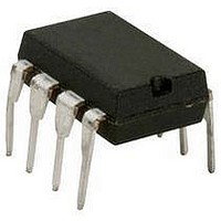
IC CONV V TO I HYBRID 38-DIP

1B21AN

Manufacturer Part Number
1B21AN
Description
IC CONV V TO I HYBRID 38-DIP
Manufacturer
Analog Devices Inc
Type
Voltage and Current Controllerr
Datasheet

Specifications of 1B21AN

Rohs Status
RoHS non-compliant
Full Scale
±50ppm/°C
Linearity
±0.02%
Mounting Type
Through Hole
Package / Case
38-DIP (0.500", 12.70mm), 8 Leads
Ic Function
Voltage To Current Converter IC
Supply Voltage Range
14.25V To 15.75V
Operating Temperature Range
-40°C To +85°C
Digital Ic Case Style
DIP
No. Of Pins
38
Lead Free Status / Rohs Status
Not Compliant

Available stocks

Company
Part Number
Manufacturer
Quantity
Price
Part Number:
1B21AN
Quantity:
1 603
Load resistance range: 0 to 1.35 kΩ maximum
Small package: 0.7” × 2.1” × 0.35”
Meets IEEE Standard 472: transient protection (SWC)
FEATURES
Wide input range: 0 V to 1 V up to 0 V to 10 V
High CMV isolation: 1500 V rms
Programmable output ranges: 4mA to 20mA
High accuracy
APPLICATIONS
Multichannel process control
DAC—current loop interface
Analog transmitters and controllers
Remote data acquisition systems
GENERAL DESCRIPTION
The 1B21 is an isolated voltage-to-current converter that
incorporates a unique circuit design utilizing transformer-based
isolation and automated surface-mount manufacturing technology.
It provides an unbeatable combination of versatility and perfor-
mance in a compact plastic package. Designed for industrial
applications, it is especially suited for harsh environments with
extremely high common-mode interference.
Functionally, the V/I converter consists of four basic sections:
input conditioning, modulator, demodulator and current source
(see Figure 1). The input is a resistor-programmable gain stage
that accepts a 0 V to 1 V up to 0 V to 10 V voltage input. This
maps into a 0 mA to 20 mA output or can be offset by 20%
using the internal reference for 4 mA to 20 mA operation. The
high level signal is modulated and passed across the barrier
which provides complete input to output galvanic isolation of
1500 V rms continuous by the use of transformer-coupling
techniques. Nonlinearity is an excellent ±0.05% maximum.
Designed for multichannel applications, the 1B21 requires an
external loop supply and can accept up to 30 V maximum. This
Rev. C
Information furnished by Analog Devices is believed to be accurate and reliable. However, no
responsibility is assumed by Analog Devices for its use, nor for any infringements of patents or other
rights of third parties that may result from its use. Specifications subject to change without notice. No
license is granted by implication or otherwise under any patent or patent rights of Analog Devices.
Trademarks and registered trademarks are the property of their respective owners.
0 to 20 mA
Low offset tempco: ±300 nA/°C
Low gain tempco: ±50 ppm/°C
Low nonlinearity: ±0.02%
High CMR: 90 dB minimum
One Technology Way, P.O. Box 9106, Norwood, MA 02062-9106, U.S.A.
Tel: 781.329.4700
Fax: 781.461.3113
provides a loop supply compliance of 27V, which is sufficient to
drive a 1.35 kΩ load resistance.
The 1B21 is fully specified over −25°C to +85°C and operates
over the industrial (−40°C to +85°C) temperature range.
DESIGN FEATURES AND USER BENEFITS
High CMV Isolation. The 1B21 features high input to output
galvanic isolation to eliminate ground loops and offer protection
against damage from transients and fault voltages. The isolation
barrier will withstand continuous CMV of 1500V rms and
meets the IEEE Standard for Transient Voltage Protection
(Std. 472-SWC).
Small Size. The 1B21 package size (0.7” × 2.1” DIP) makes it an
excellent choice in multichannel systems for maximum channel
density. The 0.35” height also facilitates applications with
limited board clearance.
Ease of Use. Complete isolated voltage-to-current conversion
with minimum external parts required to get a conditioned
current signal. No external buffers or drivers are required.
INPUT
Voltage-to-Current Converter
+15V
–15V
COM
OUT
REF
FB
18
17
19
20
22
21
REF
FUNCTIONAL BLOCK DIAGRAM
Isolated, Loop-Powered
©1991–2009 Analog Devices, Inc. All rights reserved.
TIMING
MODULATOR
OSCILLATOR
Figure 1.
ISOLATION
ISOLATION
SIGNAL
POWER
T1
T2
DEMODULATOR
RECTIFIER
TIMING
www.analog.com
1B21
1B21
38
1
OUT
HIGH
OUT
LOW

Related parts for 1B21AN

1B21AN Summary of contents

Page 1

FEATURES Wide input range High CMV isolation: 1500 V rms Programmable output ranges: 4mA to 20mA Load resistance range 1.35 kΩ maximum ...

Page 2

TABLE OF CONTENTS Features .............................................................................................. 1 Applications ....................................................................................... 1 Functional Block Diagram .............................................................. 1 General Description ......................................................................... 1 Design Features and User Benefits ................................................. 1 Revision History ............................................................................... 2 Specifications ..................................................................................... 3 Pin Configuration ............................................................................. 4 REVISION HISTORY 12/09—Rev. ...

Page 3

SPECIFICATIONS Typical at +25°C and V = ±15 V, unless otherwise noted. S Table 1. Parameter INPUT SPECIFICATIONS Input Range Full-Scale Input Input Bias Current OUTPUT SPECIFICATIONS Current Output Range Load Compliance LOOP Max Output ...

Page 4

PIN CONFIGURATION 1B21 BOTTOM VIEW Figure 2. Pin Configuration Rev Page ...

Page 5

INSIDE THE 1B21 Referring to the functional block diagram (see Figure 3), the ±15 V power inputs provide power to both the input side circuitry and the power oscillator. The 25 kHz power oscillator provides both the timing information for ...

Page 6

TC Considerations of External Resistors The specifications for gain and offset temperature coefficient (TC) for the IB21 excluded the effects of external components. The total gain TC for the circuit in Figure 4 is Gain TC = 1B21 Gain ...

Page 7

APPLICATIONS INFORMATION OUTPUT PROTECTION In many industrial applications, it may be necessary to protect the current output from accidental shorts to ac line voltages in addition to high common-mode voltages and short circuits to ground. The circuit show in Figure ...

Page 8

... PARENTHESES) ARE ROUNDED-OFF INCH EQUIVALENTS FOR REFERENCE ONLY AND ARE NOT APPROPRIATE FOR USE IN DESIGN. ORDERING GUIDE Model Temperature Range 1B21AN −25°C to +85°C ©1991–2009 Analog Devices, Inc. All rights reserved. Trademarks and registered trademarks are the property of their respective owners. 2.10 (53.34) MAX SIDE VIEW 0 ...

Related keywords