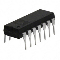
AD650JN Analog Devices Inc, AD650JN Datasheet - Page 14

AD650JN
Manufacturer Part Number
AD650JN
Description
IC V-F/F-V CONVERTER 14-DIP
Manufacturer
Analog Devices Inc
Type
Volt to Freq & Freq to Voltr
Datasheet
1.AD650KNZ.pdf
(20 pages)
Specifications of AD650JN
Mounting Type
Through Hole
Rohs Status
RoHS non-compliant
Frequency - Max
1MHz
Full Scale
±150ppm/°C
Linearity
±0.1%
Package / Case
14-DIP (0.300", 7.62mm)
Frequency
1GHz
Digital Ic Case Style
DIP
No. Of Pins
14
Peak Reflow Compatible (260 C)
No
Converter Function
VFC/FVC
Full Scale Frequency
1000
Power Supply Requirement
Dual
Single Supply Voltage (typ)
Not RequiredV
Single Supply Voltage (max)
Not RequiredV
Single Supply Voltage (min)
Not RequiredV
Dual Supply Voltage (min)
±9V
Dual Supply Voltage (max)
±18V
Operating Temperature (min)
0C
Operating Temperature (max)
70C
Operating Temperature Classification
Commercial
Package Type
PDIP
Lead Free Status / Rohs Status
Not Compliant
Available stocks
Company
Part Number
Manufacturer
Quantity
Price
Part Number:
AD650JN
Manufacturer:
AD
Quantity:
20 000
Company:
Part Number:
AD650JNZ
Manufacturer:
AD
Quantity:
1 000
Company:
Part Number:
AD650JNZ
Manufacturer:
LINEAR
Quantity:
7 838
Part Number:
AD650JNZ
Manufacturer:
ADI/亚德诺
Quantity:
20 000
AD650
100k
100
1M
100
1k
1k
10
Figure 16. Exaggerated Nonlinearity at 100 kHz Full Scale
Figure 17. Exaggerated Nonlinearity at 1 MHz Full Scale
10mV
10mV
Figure 18. PSRR vs. Full-Scale Frequency
VOLTAGE TO FREQUENCY
TRANSFER RELATION
ACTUAL
FULL SCALE FREQUENCY (Hz)
ACTUAL
10k
INPUT VOLTAGE
INPUT VOLTAGE
600ppm
100k
50ppm
IDEAL
1M
IDEAL RELATION
600ppm
10V
10V
Rev. D | Page 14 of 20
PSRR
The power supply rejection ratio is a specification of the change
in gain of the AD650 as the power supply voltage is changed.
The PSRR is expressed in units of parts-per-million change of
the gain per percent change of the power supply (ppm/%). For
example, consider a VFC with a 10 V input applied and an
output frequency of exactly 100 kHz when the power supply
potential is ±15 V. Changing the power supply to ±12.5 V is a
5 V change out of 30 V, or 16.7%. If the output frequency changes
to 99.9 kHz, then the gain has changed 0.1% or 1000 ppm. The
PSRR is 1000 ppm divided by 16.7%, which equals 60 ppm/%.
The PSRR of the AD650 is a function of the full-scale operating
frequency. At low full-scale frequencies the PSRR is determined
by the stability of the reference circuits in the device and can be
very effective. At higher frequencies, there are dynamic errors
that become more important than the static reference signals,
and consequently the PSRR is not quite as effective. The values
of PSRR are typically 0 ± 20 ppm/% at 10 kHz full-scale frequency
(R
330 pF) the PSRR is typically +80 ± 40 ppm/%, and at 1 MHz
(R
This information is summarized graphically in Figure 18.
OTHER CIRCUIT CONSIDERATIONS
The input amplifier connected to Pin 1, Pin 2, and Pin 3 is not a
standard operational amplifier. Rather, the design has been
optimized for simplicity and high speed. The single largest
difference between this amplifier and a normal op amp is the lack
of an integrator (or level shift) stage. Consequently, the voltage on
the output (Pin 1) must always be more positive than 2 V below the
inputs (Pin 2 and Pin 3). For example, in the F-to-V conversion
mode (Figure 13) the noninverting input of the op amp (Pin 2)
is grounded, which means that the output (Pin 1) is not able to
go below –2 V. Normal operation of the circuit shown in Figure 13
never calls for a negative voltage at the output, but users can
imagine an arrangement calling for a bipolar output voltage (for
example, ±10 V) by connecting an extra resistor from Pin 3 to a
positive voltage. However, this does not work.
Care should be taken under conditions where a high positive
input voltage exists at or before power up. These situations can
cause a latch up at the integrator output (Pin 1). This is a
nondestructive latch and, as such, normal operation can be
restored by cycling the power supply. Latch up can be prevented
by connecting two diodes (for example, 1N914 or 1N4148) as
shown in Figure 11, thereby preventing Pin 1 from swinging
below Pin 2.
IN
IN
= 16.9 kΩ, C
= 40 kΩ, C
OS
OS
= 3300 pF). At 100 kHz (R
= 51 pF) the PSRR is +350 ± 50 ppm/%.
IN
= 40 kΩ, C
OS
=


